C8051F226DK Silicon Laboratories Inc, C8051F226DK Datasheet - Page 85
C8051F226DK
Manufacturer Part Number
C8051F226DK
Description
DEV KIT F220/221/226/230/231/236
Manufacturer
Silicon Laboratories Inc
Type
MCUr
Datasheet
1.C8051F226DK.pdf
(146 pages)
Specifications of C8051F226DK
Contents
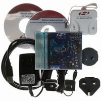
Evaluation Board, Power Supply, USB Cables, Adapter and Documentation
Processor To Be Evaluated
C8051F22x and C8051F23x
Interface Type
USB
Silicon Manufacturer
Silicon Labs
Core Architecture
8051
Silicon Core Number
C8051F226
Silicon Family Name
C8051F2xx
Lead Free Status / RoHS Status
Contains lead / RoHS non-compliant
For Use With/related Products
C8051F220, 221, 226, 230, 231, 236
Lead Free Status / Rohs Status
Lead free / RoHS Compliant
Other names
336-1241


10. Flash Memory
This MCU includes 8 k + 128 bytes of on-chip, re-programmable Flash memory for program code and non-
volatile data storage. The Flash memory can be programmed in-system, a single byte at a time, through
the JTAG interface or by software using the MOVX instruction. Once cleared to 0, a Flash bit must be
erased to set it back to 1. The bytes would typically be erased (set to 0xFF) before being reprogrammed.
The write and erase operations are automatically timed by hardware for proper execution. Data polling to
determine the end of the write/erase operation is not required. The Flash memory is designed to withstand
at least 20,000 write/erase cycles. Refer to Table 10.1 for the electrical characteristics of the Flash mem-
ory.
10.1. Programming The Flash Memory
The simplest means of programming the Flash memory is through the JTAG interface using programming
tools provided by Silicon Labs or a third party vendor. This is the only means for programming a non-ini-
tialized device. For details on the JTAG commands to program Flash memory, see Section 18.1.
The Flash memory can be programmed by software using the MOVX instruction with the address and data
byte to be programmed provided as normal operands. Before writing to Flash memory using MOVX, flash
write operations must be enabled by setting the PSWE Program Store Write Enable bit (PSCTL.0) to logic
1. Writing to Flash remains enabled until the PSWE bit is cleared by software.
To ensure the contents of the Flash contents, it is strongly recommended that the on-chip V
enabled (by tieing the MONEN pin 'high') in any application that writes and/or erases Flash memory from
software.
Writes to Flash memory can clear bits but cannot set them. Only an erase operation can set bits in Flash.
The byte location to be programmed must be erased before a new value can be written. The 8kbyte Flash
memory is organized in 512-byte sectors. The erase operation applies to an entire sector (setting all bytes
in the sector to 0xFF). Setting the PSEE Program Store Erase Enable bit (PSCTL.1) and PSWE Program
Store Write Enable bit (PSCTL.0) to logic 1 and then using the MOVX command to write a data byte to any
byte location within the sector will erase an entire 512-byte sector. The data byte written can be of any
value because it is not actually written to the Flash. Flash erasure remains enabled until the PSEE bit is
cleared by software. The following sequence illustrates the algorithm for programming the Flash memory
by software:
Write/Erase timing is automatically controlled by hardware based on the prescaler value held in the Flash
Memory Timing Prescaler register (FLSCL). The 4-bit prescaler value FLASCL determines the time inter-
val for write/erase operations. The FLASCL value required for a given system clock is shown in SFR Defi-
nition 10.2, along with the formula used to derive the FLASCL values. When FLASCL is set to 1111b, the
1. Disable interrupts.
2. Enable Flash Memory write/erase in FLSCL Register using FLASCL bits.
3. Set PSEE (PSCTL.1) to enable Flash sector erase.
4. Set PSWE (PSCTL.0) to enable Flash writes.
5. Use MOVX to write a data byte to any location within the 512-byte sector to be erased.
6. Clear PSEE to disable Flash sector erase.
7. Use MOVX to write a data byte to the desired byte location within the erased 512-byte sector.
8. Clear the PSWE bit to disable Flash writes.
Repeat until finished. (Any number of bytes can be written from a single byte to and entire
sector.)
Rev. 1.6
C8051F2xx
DD
monitor be
85
Related parts for C8051F226DK
Image
Part Number
Description
Manufacturer
Datasheet
Request
R

Part Number:
Description:
SMD/C°/SINGLE-ENDED OUTPUT SILICON OSCILLATOR
Manufacturer:
Silicon Laboratories Inc
Part Number:
Description:
Manufacturer:
Silicon Laboratories Inc
Datasheet:
Part Number:
Description:
N/A N/A/SI4010 AES KEYFOB DEMO WITH LCD RX
Manufacturer:
Silicon Laboratories Inc
Datasheet:
Part Number:
Description:
N/A N/A/SI4010 SIMPLIFIED KEY FOB DEMO WITH LED RX
Manufacturer:
Silicon Laboratories Inc
Datasheet:
Part Number:
Description:
N/A/-40 TO 85 OC/EZLINK MODULE; F930/4432 HIGH BAND (REV E/B1)
Manufacturer:
Silicon Laboratories Inc
Part Number:
Description:
EZLink Module; F930/4432 Low Band (rev e/B1)
Manufacturer:
Silicon Laboratories Inc
Part Number:
Description:
I°/4460 10 DBM RADIO TEST CARD 434 MHZ
Manufacturer:
Silicon Laboratories Inc
Part Number:
Description:
I°/4461 14 DBM RADIO TEST CARD 868 MHZ
Manufacturer:
Silicon Laboratories Inc
Part Number:
Description:
I°/4463 20 DBM RFSWITCH RADIO TEST CARD 460 MHZ
Manufacturer:
Silicon Laboratories Inc
Part Number:
Description:
I°/4463 20 DBM RADIO TEST CARD 868 MHZ
Manufacturer:
Silicon Laboratories Inc
Part Number:
Description:
I°/4463 27 DBM RADIO TEST CARD 868 MHZ
Manufacturer:
Silicon Laboratories Inc
Part Number:
Description:
I°/4463 SKYWORKS 30 DBM RADIO TEST CARD 915 MHZ
Manufacturer:
Silicon Laboratories Inc
Part Number:
Description:
N/A N/A/-40 TO 85 OC/4463 RFMD 30 DBM RADIO TEST CARD 915 MHZ
Manufacturer:
Silicon Laboratories Inc
Part Number:
Description:
I°/4463 20 DBM RADIO TEST CARD 169 MHZ
Manufacturer:
Silicon Laboratories Inc