C8051F226DK Silicon Laboratories Inc, C8051F226DK Datasheet - Page 105
C8051F226DK
Manufacturer Part Number
C8051F226DK
Description
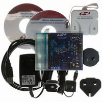
DEV KIT F220/221/226/230/231/236
Manufacturer
Silicon Laboratories Inc
Type
MCUr
Datasheet
1.C8051F226DK.pdf
(146 pages)
Specifications of C8051F226DK
Contents
Evaluation Board, Power Supply, USB Cables, Adapter and Documentation
Processor To Be Evaluated
C8051F22x and C8051F23x
Interface Type
USB
Silicon Manufacturer
Silicon Labs
Core Architecture
8051
Silicon Core Number
C8051F226
Silicon Family Name
C8051F2xx
Lead Free Status / RoHS Status
Contains lead / RoHS non-compliant
For Use With/related Products
C8051F220, 221, 226, 230, 231, 236
Lead Free Status / Rohs Status
Lead free / RoHS Compliant
Other names
336-1241


14.2. General Purpose Port I/O
Each I/O port is accessed through a corresponding special function register (SFR) that is both byte
addressable and bit addressable. When writing to a port, the value written to the SFR is latched to main-
tain the output data value at each pin. When reading, the logic levels of the port’s input pins are returned
regardless of the PRTnMX settings (i.e., even when the pin is assigned to another signal by the MUX, the
Port Register can always still read its corresponding Port I/O pin), provided its pin is configured for digital
input mode. The exception to this is the execution of the read-modify-write instructions. The read-modify-
write instructions when operating on a port SFR are the following: ANL, ORL, XRL, JBC, CPL, INC, DEC,
DJNZ and MOV, CLR or SETB, when the destination is an individual bit in a port SFR. For these instruc-
tions, the value of the register (not the pin) is read, modified, and written back to the SFR.
Bits7–0: P0.[7:0]
Bits7–0: PRT0CF.[7:0]: Output Configuration Bits for P0.7–P0.0 (respectively)
P0.7
R/W
Bit7
R/W
Bit7
(Write - Output appears on I/O pins per PRT0MX, PRT1MX, and PRT2MX Registers)
0: Logic Low Output.
1: Logic High Output (high impedance if corresponding PRT0CF.n bit = 0)
(Read - Regardless of PRT0MX, PRT1MX, and PRT2MX Register settings).
0: P0.n pin is logic low.
1: P0.n pin is logic high.
0: Corresponding P0.n Output mode is Open-Drain.
1: Corresponding P0.n Output mode is Push-Pull.
P0.6
SFR Definition 14.5. PRT0CF: Port0 Configuration Register
R/W
Bit6
R/W
Bit6
P0.5
R/W
Bit5
R/W
SFR Definition 14.4. P0: Port0 Register
Bit5
P0.4
R/W
Bit4
R/W
Bit4
P0.3
R/W
Bit3
Rev. 1.6
R/W
Bit3
P0.2
R/W
Bit2
R/W
Bit2
P0.1
R/W
Bit1
R/W
Bit1
(bit addressable)
C8051F2xx
P0.0
R/W
Bit0
R/W
Bit0
SFR Address:
SFR Address:
Reset Value
Reset Value
00000000
11111111
0x80
0xA4
105
Related parts for C8051F226DK
Image
Part Number
Description
Manufacturer
Datasheet
Request
R

Part Number:
Description:
SMD/C°/SINGLE-ENDED OUTPUT SILICON OSCILLATOR
Manufacturer:
Silicon Laboratories Inc
Part Number:
Description:
Manufacturer:
Silicon Laboratories Inc
Datasheet:
Part Number:
Description:
N/A N/A/SI4010 AES KEYFOB DEMO WITH LCD RX
Manufacturer:
Silicon Laboratories Inc
Datasheet:
Part Number:
Description:
N/A N/A/SI4010 SIMPLIFIED KEY FOB DEMO WITH LED RX
Manufacturer:
Silicon Laboratories Inc
Datasheet:
Part Number:
Description:
N/A/-40 TO 85 OC/EZLINK MODULE; F930/4432 HIGH BAND (REV E/B1)
Manufacturer:
Silicon Laboratories Inc
Part Number:
Description:
EZLink Module; F930/4432 Low Band (rev e/B1)
Manufacturer:
Silicon Laboratories Inc
Part Number:
Description:
I°/4460 10 DBM RADIO TEST CARD 434 MHZ
Manufacturer:
Silicon Laboratories Inc
Part Number:
Description:
I°/4461 14 DBM RADIO TEST CARD 868 MHZ
Manufacturer:
Silicon Laboratories Inc
Part Number:
Description:
I°/4463 20 DBM RFSWITCH RADIO TEST CARD 460 MHZ
Manufacturer:
Silicon Laboratories Inc
Part Number:
Description:
I°/4463 20 DBM RADIO TEST CARD 868 MHZ
Manufacturer:
Silicon Laboratories Inc
Part Number:
Description:
I°/4463 27 DBM RADIO TEST CARD 868 MHZ
Manufacturer:
Silicon Laboratories Inc
Part Number:
Description:
I°/4463 SKYWORKS 30 DBM RADIO TEST CARD 915 MHZ
Manufacturer:
Silicon Laboratories Inc
Part Number:
Description:
N/A N/A/-40 TO 85 OC/4463 RFMD 30 DBM RADIO TEST CARD 915 MHZ
Manufacturer:
Silicon Laboratories Inc
Part Number:
Description:
I°/4463 20 DBM RADIO TEST CARD 169 MHZ
Manufacturer:
Silicon Laboratories Inc