C8051F226DK Silicon Laboratories Inc, C8051F226DK Datasheet - Page 20
C8051F226DK
Manufacturer Part Number
C8051F226DK
Description
DEV KIT F220/221/226/230/231/236
Manufacturer
Silicon Laboratories Inc
Type
MCUr
Datasheet
1.C8051F226DK.pdf
(146 pages)
Specifications of C8051F226DK
Contents
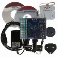
Evaluation Board, Power Supply, USB Cables, Adapter and Documentation
Processor To Be Evaluated
C8051F22x and C8051F23x
Interface Type
USB
Silicon Manufacturer
Silicon Labs
Core Architecture
8051
Silicon Core Number
C8051F226
Silicon Family Name
C8051F2xx
Lead Free Status / RoHS Status
Contains lead / RoHS non-compliant
For Use With/related Products
C8051F220, 221, 226, 230, 231, 236
Lead Free Status / Rohs Status
Lead free / RoHS Compliant
Other names
336-1241


C8051F2xx
1.5.
The C8051F206, C8051F220/1/6 and C8051F230/1/6 include a Full-Duplex UART and SPI Bus. Each of
the serial buses is fully implemented in hardware and makes extensive use of the CIP-51's interrupts, thus
requiring very little intervention by the CPU. The serial buses do not have to "share" resources such as
timers, interrupts, or Port I/O, so both of the serial buses may be used simultaneously. (You may use
Timer1, Timer 2, or SYSCLK to generate baud rates for UART).
1.6.
The C8051F220/1/6 has an on-chip 8-bit SAR ADC and the C8051F206 has a 12-bit SAR ADC with a pro-
grammable gain amplifier. With a maximum throughput of 100ksps, the ADC offers true 8-bit with an INL of
±1/4 LSB, and or 12-bit accuracy with ±2 LSB. The voltage reference can be the power supply (
an external reference voltage (VREF). Also, the system controller can place the ADC into a power-saving
shutdown mode when not in use. A programmable gain amplifier follows the analog multiplexer. The gain
can be set in software from 0.5 to 16 in powers of 2.
Conversions can be initiated in two ways; a software command or an overflow on Timer 2. This flexibility
allows the start of conversion to be triggered by software events, or convert continuously. A completed
conversion causes an interrupt, or a status bit can be polled in software to determine the end of conver-
sion. The resulting 8-bit data word is latched into an SFR upon completion of a conversion.
20
Comparators
INT0 & INT1
Serial Ports
Analog to Digital Converter
ADC
T0,T1,T2
SYSCLK
External
Timers
UART
0 & 1
SPI
Figure 1.9. Port I/O Functional Block Diagram
M
A
U
X
Registers
PRTnMX
MUX
MUX
Port
MUX
Port
Port
0
1
2
Rev. 1.6
Port0 I/O Cell
Port1 I/O Cell
Port2 I/O Cell
Port3 I/O Cell
PRTnCF &
PnMODE
registers
External
P0.0/TX
P0.1/RX
P0.2/INT0
P0.3/INT1
P0.4/T0
P0.5/T1
P0.6/T2
P0.7/T2EX
P1.0/CP0+
P1.1/CP0-
P1.2/CP0
P1.3/CP1+
P1.4/CP1-
P1.5/CP1
P1.6/SYSCLK
P1.7
P2.0/SCK
P2.1/MISO
P2.2/MOSI
P2.3/NSS
P2.4
P2.5
P2.6
P2.7
P3.0
P3.1
P3.2
P3.3
P3.4
P3.5
P3.6
P3.7
pins
configured via software as an
analog input to the ADC
Any port pin may be
V
DD ), or
Related parts for C8051F226DK
Image
Part Number
Description
Manufacturer
Datasheet
Request
R

Part Number:
Description:
SMD/C°/SINGLE-ENDED OUTPUT SILICON OSCILLATOR
Manufacturer:
Silicon Laboratories Inc
Part Number:
Description:
Manufacturer:
Silicon Laboratories Inc
Datasheet:
Part Number:
Description:
N/A N/A/SI4010 AES KEYFOB DEMO WITH LCD RX
Manufacturer:
Silicon Laboratories Inc
Datasheet:
Part Number:
Description:
N/A N/A/SI4010 SIMPLIFIED KEY FOB DEMO WITH LED RX
Manufacturer:
Silicon Laboratories Inc
Datasheet:
Part Number:
Description:
N/A/-40 TO 85 OC/EZLINK MODULE; F930/4432 HIGH BAND (REV E/B1)
Manufacturer:
Silicon Laboratories Inc
Part Number:
Description:
EZLink Module; F930/4432 Low Band (rev e/B1)
Manufacturer:
Silicon Laboratories Inc
Part Number:
Description:
I°/4460 10 DBM RADIO TEST CARD 434 MHZ
Manufacturer:
Silicon Laboratories Inc
Part Number:
Description:
I°/4461 14 DBM RADIO TEST CARD 868 MHZ
Manufacturer:
Silicon Laboratories Inc
Part Number:
Description:
I°/4463 20 DBM RFSWITCH RADIO TEST CARD 460 MHZ
Manufacturer:
Silicon Laboratories Inc
Part Number:
Description:
I°/4463 20 DBM RADIO TEST CARD 868 MHZ
Manufacturer:
Silicon Laboratories Inc
Part Number:
Description:
I°/4463 27 DBM RADIO TEST CARD 868 MHZ
Manufacturer:
Silicon Laboratories Inc
Part Number:
Description:
I°/4463 SKYWORKS 30 DBM RADIO TEST CARD 915 MHZ
Manufacturer:
Silicon Laboratories Inc
Part Number:
Description:
N/A N/A/-40 TO 85 OC/4463 RFMD 30 DBM RADIO TEST CARD 915 MHZ
Manufacturer:
Silicon Laboratories Inc
Part Number:
Description:
I°/4463 20 DBM RADIO TEST CARD 169 MHZ
Manufacturer:
Silicon Laboratories Inc