C8051F226DK Silicon Laboratories Inc, C8051F226DK Datasheet - Page 91
C8051F226DK
Manufacturer Part Number
C8051F226DK
Description
DEV KIT F220/221/226/230/231/236
Manufacturer
Silicon Laboratories Inc
Type
MCUr
Datasheet
1.C8051F226DK.pdf
(146 pages)
Specifications of C8051F226DK
Contents
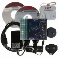
Evaluation Board, Power Supply, USB Cables, Adapter and Documentation
Processor To Be Evaluated
C8051F22x and C8051F23x
Interface Type
USB
Silicon Manufacturer
Silicon Labs
Core Architecture
8051
Silicon Core Number
C8051F226
Silicon Family Name
C8051F2xx
Lead Free Status / RoHS Status
Contains lead / RoHS non-compliant
For Use With/related Products
C8051F220, 221, 226, 230, 231, 236
Lead Free Status / Rohs Status
Lead free / RoHS Compliant
Other names
336-1241


12. Reset Sources
The reset circuitry of the MCU allows the controller to be easily placed in a predefined default condition.
On entry to this reset state, the CIP-51 halts program execution, forces the external port pins to a known
state and initializes the SFRs to their defined reset values. Interrupts and timers are disabled. On exit, the
program counter (PC) is reset, and program execution starts at location 0x0000.
All of the SFRs are reset to predefined values. The reset values of the SFR bits are defined in the SFR
detailed descriptions. The contents of internal data memory are not changed during a reset and any previ-
ously stored data is preserved. However, since the stack pointer SFR is reset, the stack is effectively lost
even though the data on the stack are not altered.
The I/O port latches are reset to 0xFF (all logic ones), activating internal weak pull-ups which take the
external I/O pins to a high state. The weak pull-ups are enabled during and after the reset. If the source of
reset is from the V
V
On exit from the reset state, the MCU uses the internal oscillator running at 2MHz as the system clock by
default. Refer to Section 13 for information on selecting and configuring the system clock source. The
Watchdog Timer is enabled using its longest timeout interval. (Section 12.7 details the use of the Watch-
dog Timer.) Once the system clock source is stable, program execution begins at location 0x0000.
There are six sources for putting the MCU into the reset state: power-on/power-fail (V
RST pin, software commanded, Comparator 0, Missing Clock Detector, and Watchdog Timer. Each reset
source is described below:
DD
CP0+
CP0-
reset timeout.
System
DD
Clock
Monitor or writing a '1' to the PORSF bit, the RST pin is driven low until the end of the
Comparator 0
+
-
Detector
Missing
Clock
EN
Figure 12.1. Reset Sources Diagram
C0RSEF
EN
WDT
PRE
Rev. 1.6
VDD
CIP-51
Core
(Software Reset)
SWRSF
MonEn
Supply
Monitor
+
-
System Reset
Timeout
Supply
Reset
(wired-OR)
C8051F2xx
Reset
Funnel
DD
monitor), external
/RST
91
Related parts for C8051F226DK
Image
Part Number
Description
Manufacturer
Datasheet
Request
R

Part Number:
Description:
SMD/C°/SINGLE-ENDED OUTPUT SILICON OSCILLATOR
Manufacturer:
Silicon Laboratories Inc
Part Number:
Description:
Manufacturer:
Silicon Laboratories Inc
Datasheet:
Part Number:
Description:
N/A N/A/SI4010 AES KEYFOB DEMO WITH LCD RX
Manufacturer:
Silicon Laboratories Inc
Datasheet:
Part Number:
Description:
N/A N/A/SI4010 SIMPLIFIED KEY FOB DEMO WITH LED RX
Manufacturer:
Silicon Laboratories Inc
Datasheet:
Part Number:
Description:
N/A/-40 TO 85 OC/EZLINK MODULE; F930/4432 HIGH BAND (REV E/B1)
Manufacturer:
Silicon Laboratories Inc
Part Number:
Description:
EZLink Module; F930/4432 Low Band (rev e/B1)
Manufacturer:
Silicon Laboratories Inc
Part Number:
Description:
I°/4460 10 DBM RADIO TEST CARD 434 MHZ
Manufacturer:
Silicon Laboratories Inc
Part Number:
Description:
I°/4461 14 DBM RADIO TEST CARD 868 MHZ
Manufacturer:
Silicon Laboratories Inc
Part Number:
Description:
I°/4463 20 DBM RFSWITCH RADIO TEST CARD 460 MHZ
Manufacturer:
Silicon Laboratories Inc
Part Number:
Description:
I°/4463 20 DBM RADIO TEST CARD 868 MHZ
Manufacturer:
Silicon Laboratories Inc
Part Number:
Description:
I°/4463 27 DBM RADIO TEST CARD 868 MHZ
Manufacturer:
Silicon Laboratories Inc
Part Number:
Description:
I°/4463 SKYWORKS 30 DBM RADIO TEST CARD 915 MHZ
Manufacturer:
Silicon Laboratories Inc
Part Number:
Description:
N/A N/A/-40 TO 85 OC/4463 RFMD 30 DBM RADIO TEST CARD 915 MHZ
Manufacturer:
Silicon Laboratories Inc
Part Number:
Description:
I°/4463 20 DBM RADIO TEST CARD 169 MHZ
Manufacturer:
Silicon Laboratories Inc