C8051F226DK Silicon Laboratories Inc, C8051F226DK Datasheet - Page 3
C8051F226DK
Manufacturer Part Number
C8051F226DK
Description
DEV KIT F220/221/226/230/231/236
Manufacturer
Silicon Laboratories Inc
Type
MCUr
Datasheet
1.C8051F226DK.pdf
(146 pages)
Specifications of C8051F226DK
Contents
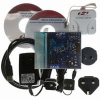
Evaluation Board, Power Supply, USB Cables, Adapter and Documentation
Processor To Be Evaluated
C8051F22x and C8051F23x
Interface Type
USB
Silicon Manufacturer
Silicon Labs
Core Architecture
8051
Silicon Core Number
C8051F226
Silicon Family Name
C8051F2xx
Lead Free Status / RoHS Status
Contains lead / RoHS non-compliant
For Use With/related Products
C8051F220, 221, 226, 230, 231, 236
Lead Free Status / Rohs Status
Lead free / RoHS Compliant
Other names
336-1241


Table of Contents
1. System Overview.................................................................................................... 11
2. Absolute Maximum Ratings .................................................................................. 23
3. Global DC Electrical Characteristics .................................................................... 24
4. Pinout and Package Definitions............................................................................ 25
5. ADC (8-Bit, C8051F220/1/6 Only)........................................................................... 32
6. ADC (12-Bit, C8051F206 Only)............................................................................... 40
7. Voltage Reference (C8051F206/220/221/226) ....................................................... 50
8. Comparators ........................................................................................................... 52
9. CIP-51 Microcontroller ........................................................................................... 58
1.1. CIP-51TM Microcontroller Core ........................................................................ 15
1.2. On-Board Memory ............................................................................................ 17
1.3. JTAG
1.4. Digital/Analog Configurable I/O......................................................................... 19
1.5. Serial Ports ....................................................................................................... 20
1.6. Analog to Digital Converter ............................................................................... 20
1.7. Comparators ..................................................................................................... 21
5.1. Analog Multiplexer and PGA............................................................................. 32
5.2. ADC Modes of Operation.................................................................................. 33
5.3. ADC Programmable Window Detector ............................................................. 37
6.1. Analog Multiplexer and PGA............................................................................. 40
6.2. ADC Modes of Operation.................................................................................. 41
6.3. ADC Programmable Window Detector ............................................................. 46
9.1. Instruction Set ................................................................................................... 60
9.2. Memory Organization........................................................................................ 65
9.3. Special Function Registers ............................................................................... 68
9.4. Interrupt Handler ............................................................................................... 74
1.1.1. Fully 8051 Compatible.............................................................................. 15
1.1.2. Improved Throughput ............................................................................... 15
1.1.3. Additional Features .................................................................................. 16
9.1.1. Instruction and CPU Timing ..................................................................... 60
9.1.2. MOVX Instruction and Program Memory ................................................. 60
9.2.1. Program Memory...................................................................................... 65
9.2.2. Data Memory............................................................................................ 65
9.2.3. General Purpose Registers ...................................................................... 66
9.2.4. Bit Addressable Locations........................................................................ 66
9.2.5. Stack ....................................................................................................... 67
9.3.1. Register Descriptions ............................................................................... 71
9.4.1. MCU Interrupt Sources and Vectors ........................................................ 74
9.4.2. External Interrupts .................................................................................... 74
9.4.3. Software Controlled Interrupts.................................................................. 74
9.4.4. Interrupt Priorities ..................................................................................... 76
9.4.5. Interrupt Latency ...................................................................................... 76
9.4.6. Interrupt Register Descriptions................................................................. 77
............................................................................................................ 18
Rev. 1.6
C8051F2xx
3
Related parts for C8051F226DK
Image
Part Number
Description
Manufacturer
Datasheet
Request
R

Part Number:
Description:
SMD/C°/SINGLE-ENDED OUTPUT SILICON OSCILLATOR
Manufacturer:
Silicon Laboratories Inc
Part Number:
Description:
Manufacturer:
Silicon Laboratories Inc
Datasheet:
Part Number:
Description:
N/A N/A/SI4010 AES KEYFOB DEMO WITH LCD RX
Manufacturer:
Silicon Laboratories Inc
Datasheet:
Part Number:
Description:
N/A N/A/SI4010 SIMPLIFIED KEY FOB DEMO WITH LED RX
Manufacturer:
Silicon Laboratories Inc
Datasheet:
Part Number:
Description:
N/A/-40 TO 85 OC/EZLINK MODULE; F930/4432 HIGH BAND (REV E/B1)
Manufacturer:
Silicon Laboratories Inc
Part Number:
Description:
EZLink Module; F930/4432 Low Band (rev e/B1)
Manufacturer:
Silicon Laboratories Inc
Part Number:
Description:
I°/4460 10 DBM RADIO TEST CARD 434 MHZ
Manufacturer:
Silicon Laboratories Inc
Part Number:
Description:
I°/4461 14 DBM RADIO TEST CARD 868 MHZ
Manufacturer:
Silicon Laboratories Inc
Part Number:
Description:
I°/4463 20 DBM RFSWITCH RADIO TEST CARD 460 MHZ
Manufacturer:
Silicon Laboratories Inc
Part Number:
Description:
I°/4463 20 DBM RADIO TEST CARD 868 MHZ
Manufacturer:
Silicon Laboratories Inc
Part Number:
Description:
I°/4463 27 DBM RADIO TEST CARD 868 MHZ
Manufacturer:
Silicon Laboratories Inc
Part Number:
Description:
I°/4463 SKYWORKS 30 DBM RADIO TEST CARD 915 MHZ
Manufacturer:
Silicon Laboratories Inc
Part Number:
Description:
N/A N/A/-40 TO 85 OC/4463 RFMD 30 DBM RADIO TEST CARD 915 MHZ
Manufacturer:
Silicon Laboratories Inc
Part Number:
Description:
I°/4463 20 DBM RADIO TEST CARD 169 MHZ
Manufacturer:
Silicon Laboratories Inc