C8051F226DK Silicon Laboratories Inc, C8051F226DK Datasheet - Page 15
C8051F226DK
Manufacturer Part Number
C8051F226DK
Description
DEV KIT F220/221/226/230/231/236
Manufacturer
Silicon Laboratories Inc
Type
MCUr
Datasheet
1.C8051F226DK.pdf
(146 pages)
Specifications of C8051F226DK
Contents
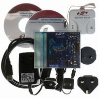
Evaluation Board, Power Supply, USB Cables, Adapter and Documentation
Processor To Be Evaluated
C8051F22x and C8051F23x
Interface Type
USB
Silicon Manufacturer
Silicon Labs
Core Architecture
8051
Silicon Core Number
C8051F226
Silicon Family Name
C8051F2xx
Lead Free Status / RoHS Status
Contains lead / RoHS non-compliant
For Use With/related Products
C8051F220, 221, 226, 230, 231, 236
Lead Free Status / Rohs Status
Lead free / RoHS Compliant
Other names
336-1241


1.1.
1.1.1. Fully 8051 Compatible
The C8051F206, C8051F220/1/6 and C8051F230/1/6 utilize Silcon Labs’ proprietary CIP-51 microcon-
troller core. The CIP-51 is fully compatible with the MCS-51
assemblers and compilers can be used to develop software. The core contains the peripherals included
with a standard 8052, including three 16-bit counter/timers, a full-duplex UART, 256 bytes of internal RAM,
an optional 1024 bytes of XRAM, 128 byte Special Function Register (SFR) address space, and four byte-
wide I/O Ports.
1.1.2. Improved Throughput
The CIP-51 employs a pipelined architecture that greatly increases its instruction throughput over the stan-
dard 8051 architecture. In a standard 8051, all instructions except for MUL and DIV take 12 or 24 system
clock cycles to execute with a maximum system clock of 12 MHz. By contrast, the CIP-51 core executes
70% of its instructions in one or two system clock cycles, with only four instructions taking more than four
system clock cycles.
The CIP-51 has a total of 109 instructions. The number of instructions versus the system clock cycles to
execute them is as follows:
Clocks to Execute
XTAL1
XTAL2
/RST
VDD
GND
TCK
TMS
TDI
TDO
Instructions
NC
CIP-51
Digital Power
TM
Oscillator
Oscillator
Monitor,
External
Internal
Circuit
JTAG
Logic
WDT
VDD
Microcontroller Core
Figure 1.4. C8051F231 Block Diagram (32 LQFP)
Emulation HW
26
1
System Clock
Reset
C
50
o
8
0
5
1
e
r
2
SFR Bus
256 byte
Clock & Reset
FLASH
Configuration
8kbyte
SRAM
2/3
5
Rev. 1.6
14
3
TM
3/4
CP0
CP1
7
Comparator
Port Mux
Port I/O Mode
Timer 0
Timer 1
Timer 2
Control
Port 0
UART
Port 1
Port 2
Port 3
Latch
Latch
Latch
Latch
Config.
& Config.
SPI
instruction set. Standard 803x/805x
CP0
CP1
CP0+
CP0-
CP1+
CP1-
3
4
M
M
M
P
U
X
P
U
X
P
U
X
0
1
2
C8051F2xx
4/5
1
P
D
P
D
P
D
0
v
1
v
2
v
r
r
r
2
5
P0.0/TX
P0.1/RX
P0.2//INT0
P0.3//INT1
P0.4/T0
P0.5/T1
P0.6/T2
P0.7/T2EX
P1.0/CP0+
P1.1/CP0-
P1.2/CP0
P1.3/CP1+
P1.4/CP1-
P1.5/CP1
P1.6/SYSCLK
P1.7
P2.0/SCK
P2.1/MISO
P2.2/MOSI
P2.3/NSS
P2.4
P2.5
1
8
15
Related parts for C8051F226DK
Image
Part Number
Description
Manufacturer
Datasheet
Request
R

Part Number:
Description:
SMD/C°/SINGLE-ENDED OUTPUT SILICON OSCILLATOR
Manufacturer:
Silicon Laboratories Inc
Part Number:
Description:
Manufacturer:
Silicon Laboratories Inc
Datasheet:
Part Number:
Description:
N/A N/A/SI4010 AES KEYFOB DEMO WITH LCD RX
Manufacturer:
Silicon Laboratories Inc
Datasheet:
Part Number:
Description:
N/A N/A/SI4010 SIMPLIFIED KEY FOB DEMO WITH LED RX
Manufacturer:
Silicon Laboratories Inc
Datasheet:
Part Number:
Description:
N/A/-40 TO 85 OC/EZLINK MODULE; F930/4432 HIGH BAND (REV E/B1)
Manufacturer:
Silicon Laboratories Inc
Part Number:
Description:
EZLink Module; F930/4432 Low Band (rev e/B1)
Manufacturer:
Silicon Laboratories Inc
Part Number:
Description:
I°/4460 10 DBM RADIO TEST CARD 434 MHZ
Manufacturer:
Silicon Laboratories Inc
Part Number:
Description:
I°/4461 14 DBM RADIO TEST CARD 868 MHZ
Manufacturer:
Silicon Laboratories Inc
Part Number:
Description:
I°/4463 20 DBM RFSWITCH RADIO TEST CARD 460 MHZ
Manufacturer:
Silicon Laboratories Inc
Part Number:
Description:
I°/4463 20 DBM RADIO TEST CARD 868 MHZ
Manufacturer:
Silicon Laboratories Inc
Part Number:
Description:
I°/4463 27 DBM RADIO TEST CARD 868 MHZ
Manufacturer:
Silicon Laboratories Inc
Part Number:
Description:
I°/4463 SKYWORKS 30 DBM RADIO TEST CARD 915 MHZ
Manufacturer:
Silicon Laboratories Inc
Part Number:
Description:
N/A N/A/-40 TO 85 OC/4463 RFMD 30 DBM RADIO TEST CARD 915 MHZ
Manufacturer:
Silicon Laboratories Inc
Part Number:
Description:
I°/4463 20 DBM RADIO TEST CARD 169 MHZ
Manufacturer:
Silicon Laboratories Inc