C8051F226DK Silicon Laboratories Inc, C8051F226DK Datasheet - Page 76
C8051F226DK
Manufacturer Part Number
C8051F226DK
Description
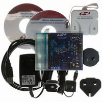
DEV KIT F220/221/226/230/231/236
Manufacturer
Silicon Laboratories Inc
Type
MCUr
Datasheet
1.C8051F226DK.pdf
(146 pages)
Specifications of C8051F226DK
Contents
Evaluation Board, Power Supply, USB Cables, Adapter and Documentation
Processor To Be Evaluated
C8051F22x and C8051F23x
Interface Type
USB
Silicon Manufacturer
Silicon Labs
Core Architecture
8051
Silicon Core Number
C8051F226
Silicon Family Name
C8051F2xx
Lead Free Status / RoHS Status
Contains lead / RoHS non-compliant
For Use With/related Products
C8051F220, 221, 226, 230, 231, 236
Lead Free Status / Rohs Status
Lead free / RoHS Compliant
Other names
336-1241


C8051F2xx
9.4.4. Interrupt Priorities
Each interrupt source can be individually programmed to one of two priority levels: low or high. A low prior-
ity interrupt service routine can be preempted by a high priority interrupt. A high priority interrupt cannot be
preempted. Each interrupt has an associated interrupt priority bit in an SFR (IP–EIP2) used to configure its
priority level. Low priority is the default. If two interrupts are recognized simultaneously, the interrupt with
the higher priority is serviced first. If both interrupts have the same priority level, a fixed priority order is
used to arbitrate.
9.4.5. Interrupt Latency
Interrupt response time depends on the state of the CPU when the interrupt occurs. Pending interrupts are
sampled and priority decoded each system clock cycle. Therefore, the fastest possible response time is 5
system clock cycles: 1 clock cycle to detect the interrupt and 4 clock cycles to complete the LCALL to the
ISR. If an interrupt is pending when a RETI is executed, a single instruction is executed before an LCALL
is made to service the pending interrupt. Therefore, the maximum response time for an interrupt (when no
other interrupt is currently being serviced or the new interrupt is of greater priority) occurs when the CPU is
performing an RETI instruction followed by a DIV as the next instruction. In this case, the response time is
18 system clock cycles: 1 clock cycle to detect the interrupt, 5 clock cycles to execute the RETI, 8 clock
cycles to complete the DIV instruction and 4 clock cycles to execute the LCALL to the ISR. NOTE: If a
Flash write or erase is performed, the MCU is stalled during the operation and interrupts will not be ser-
viced until the operation is complete. If the CPU is executing an ISR for an interrupt with equal or higher
priority, the new interrupt will not be serviced until the current ISR completes, including the RETI and fol-
lowing instruction.
76
ADC0 End of Conversion
Software Controlled Interrupt 0
Software Controlled Interrupt 1
Software Controlled Interrupt 2
Software Controlled Interrupt 3
Unused Interrupt Location
External Crystal OSC Ready
Interrupt Source
Table 9.4. Interrupt Summary (Continued)
Interrupt
0x00AB
0x007B
0x008B
0x009B
0x00A3
0x0083
0x0093
Vector
Priority
Order
15
16
17
18
19
20
21
Rev. 1.6
ADCINT (ADC0CN.5)
SCI0 (SWCINT.4)
SCI1 (SWCINT.5)
SCI2 (SWCINT.6)
SCI3 (SWCINT.7)
None
XTLVLD (OSCXCN.7)
Interrupt-Pending Flag
Reserved (EIE2.6)
EADC0 (EIE2.1)
EXVLD (EIE2.7)
ESCI0 (EIE2.2)
ESCI1 (EIE2.3)
ESCI2 (EIE2.4)
ESCI3 (EIE2.5)
Enable
Related parts for C8051F226DK
Image
Part Number
Description
Manufacturer
Datasheet
Request
R

Part Number:
Description:
SMD/C°/SINGLE-ENDED OUTPUT SILICON OSCILLATOR
Manufacturer:
Silicon Laboratories Inc
Part Number:
Description:
Manufacturer:
Silicon Laboratories Inc
Datasheet:
Part Number:
Description:
N/A N/A/SI4010 AES KEYFOB DEMO WITH LCD RX
Manufacturer:
Silicon Laboratories Inc
Datasheet:
Part Number:
Description:
N/A N/A/SI4010 SIMPLIFIED KEY FOB DEMO WITH LED RX
Manufacturer:
Silicon Laboratories Inc
Datasheet:
Part Number:
Description:
N/A/-40 TO 85 OC/EZLINK MODULE; F930/4432 HIGH BAND (REV E/B1)
Manufacturer:
Silicon Laboratories Inc
Part Number:
Description:
EZLink Module; F930/4432 Low Band (rev e/B1)
Manufacturer:
Silicon Laboratories Inc
Part Number:
Description:
I°/4460 10 DBM RADIO TEST CARD 434 MHZ
Manufacturer:
Silicon Laboratories Inc
Part Number:
Description:
I°/4461 14 DBM RADIO TEST CARD 868 MHZ
Manufacturer:
Silicon Laboratories Inc
Part Number:
Description:
I°/4463 20 DBM RFSWITCH RADIO TEST CARD 460 MHZ
Manufacturer:
Silicon Laboratories Inc
Part Number:
Description:
I°/4463 20 DBM RADIO TEST CARD 868 MHZ
Manufacturer:
Silicon Laboratories Inc
Part Number:
Description:
I°/4463 27 DBM RADIO TEST CARD 868 MHZ
Manufacturer:
Silicon Laboratories Inc
Part Number:
Description:
I°/4463 SKYWORKS 30 DBM RADIO TEST CARD 915 MHZ
Manufacturer:
Silicon Laboratories Inc
Part Number:
Description:
N/A N/A/-40 TO 85 OC/4463 RFMD 30 DBM RADIO TEST CARD 915 MHZ
Manufacturer:
Silicon Laboratories Inc
Part Number:
Description:
I°/4463 20 DBM RADIO TEST CARD 169 MHZ
Manufacturer:
Silicon Laboratories Inc