C8051F226DK Silicon Laboratories Inc, C8051F226DK Datasheet - Page 66
C8051F226DK
Manufacturer Part Number
C8051F226DK
Description
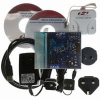
DEV KIT F220/221/226/230/231/236
Manufacturer
Silicon Laboratories Inc
Type
MCUr
Datasheet
1.C8051F226DK.pdf
(146 pages)
Specifications of C8051F226DK
Contents
Evaluation Board, Power Supply, USB Cables, Adapter and Documentation
Processor To Be Evaluated
C8051F22x and C8051F23x
Interface Type
USB
Silicon Manufacturer
Silicon Labs
Core Architecture
8051
Silicon Core Number
C8051F226
Silicon Family Name
C8051F2xx
Lead Free Status / RoHS Status
Contains lead / RoHS non-compliant
For Use With/related Products
C8051F220, 221, 226, 230, 231, 236
Lead Free Status / Rohs Status
Lead free / RoHS Compliant
Other names
336-1241


C8051F2xx
9.2.3. General Purpose Registers
The lower 32 bytes of data memory, locations 0x00 through 0x1F, may be addressed as four banks of gen-
eral-purpose registers. Each bank consists of eight byte-wide registers designated R0 through R7. Only
one of these banks may be enabled at a time. Two bits in the program status word, RS0 (PSW.3) and RS1
(PSW.4), select the active register bank (see description of the PSW in SFR Definition 9.4). This allows
fast context switching when entering subroutines and interrupt service routines. Indirect addressing
modes use registers R0 and R1 as index registers.
9.2.4. Bit Addressable Locations
In addition to direct access to data memory organized as bytes, the sixteen data memory locations at 0x20
through 0x2F are also accessible as 128 individually addressable bits. Each bit has a bit address from
0x00 to 0x7F. Bit 0 of the byte at 0x20 has bit address 0x00 while bit 7 of the byte at 0x20 has bit address
0x07. Bit 7 of the byte at 0x2F has bit address 0x7F. A bit access is distinguished from a full byte access
by the type of instruction used (bit source or destination operands as opposed to a byte source or destina-
tion).
The MCS-51™ assembly language allows an alternate notation for bit addressing of the form XX.B where
XX is the byte address and B is the bit position within the byte. For example, the instruction:
moves the Boolean value at 0x13 (bit 3 of the byte at location 0x22) into the user Carry flag.
66
0x1DFF
0x1FFF
0x207F
0x1E00
0x2000
0x0000
MOV
PROGRAM MEMORY
Programmable in 512
128 Byte ISP FLASH
C, 22h.3
Byte Sectors)
RESERVED
(In-System
FLASH
Figure 9.2. Memory Map
0x3FF
0x000
0xFF
0x7F
0x2F
0x1F
0x80
0x30
0x20
0x00
Rev. 1.6
(Indirect Addressing
(Direct and Indirect
General Purpose
Upper 128 RAM
Bit Addressable
Addressing)
1024 Byte
Registers
XRAM
Only)
DATA MEMORY
(Direct Addressing Only)
(C8051F226/236/206 only)
Special Function
External Data Memory
Lower 128 RAM
(Direct and Indirect
Addressing)
Register's
Mapped into
Space
Related parts for C8051F226DK
Image
Part Number
Description
Manufacturer
Datasheet
Request
R

Part Number:
Description:
SMD/C°/SINGLE-ENDED OUTPUT SILICON OSCILLATOR
Manufacturer:
Silicon Laboratories Inc
Part Number:
Description:
Manufacturer:
Silicon Laboratories Inc
Datasheet:
Part Number:
Description:
N/A N/A/SI4010 AES KEYFOB DEMO WITH LCD RX
Manufacturer:
Silicon Laboratories Inc
Datasheet:
Part Number:
Description:
N/A N/A/SI4010 SIMPLIFIED KEY FOB DEMO WITH LED RX
Manufacturer:
Silicon Laboratories Inc
Datasheet:
Part Number:
Description:
N/A/-40 TO 85 OC/EZLINK MODULE; F930/4432 HIGH BAND (REV E/B1)
Manufacturer:
Silicon Laboratories Inc
Part Number:
Description:
EZLink Module; F930/4432 Low Band (rev e/B1)
Manufacturer:
Silicon Laboratories Inc
Part Number:
Description:
I°/4460 10 DBM RADIO TEST CARD 434 MHZ
Manufacturer:
Silicon Laboratories Inc
Part Number:
Description:
I°/4461 14 DBM RADIO TEST CARD 868 MHZ
Manufacturer:
Silicon Laboratories Inc
Part Number:
Description:
I°/4463 20 DBM RFSWITCH RADIO TEST CARD 460 MHZ
Manufacturer:
Silicon Laboratories Inc
Part Number:
Description:
I°/4463 20 DBM RADIO TEST CARD 868 MHZ
Manufacturer:
Silicon Laboratories Inc
Part Number:
Description:
I°/4463 27 DBM RADIO TEST CARD 868 MHZ
Manufacturer:
Silicon Laboratories Inc
Part Number:
Description:
I°/4463 SKYWORKS 30 DBM RADIO TEST CARD 915 MHZ
Manufacturer:
Silicon Laboratories Inc
Part Number:
Description:
N/A N/A/-40 TO 85 OC/4463 RFMD 30 DBM RADIO TEST CARD 915 MHZ
Manufacturer:
Silicon Laboratories Inc
Part Number:
Description:
I°/4463 20 DBM RADIO TEST CARD 169 MHZ
Manufacturer:
Silicon Laboratories Inc