C8051F226DK Silicon Laboratories Inc, C8051F226DK Datasheet - Page 52
C8051F226DK
Manufacturer Part Number
C8051F226DK
Description
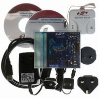
DEV KIT F220/221/226/230/231/236
Manufacturer
Silicon Laboratories Inc
Type
MCUr
Datasheet
1.C8051F226DK.pdf
(146 pages)
Specifications of C8051F226DK
Contents
Evaluation Board, Power Supply, USB Cables, Adapter and Documentation
Processor To Be Evaluated
C8051F22x and C8051F23x
Interface Type
USB
Silicon Manufacturer
Silicon Labs
Core Architecture
8051
Silicon Core Number
C8051F226
Silicon Family Name
C8051F2xx
Lead Free Status / RoHS Status
Contains lead / RoHS non-compliant
For Use With/related Products
C8051F220, 221, 226, 230, 231, 236
Lead Free Status / Rohs Status
Lead free / RoHS Compliant
Other names
336-1241


C8051F2xx
8.
Comparators
The MCU has two on-board voltage comparators as shown in Figure 8.1. The inputs of each Comparator
are available at the package pins. The output of each comparator is optionally available at port1 by config-
uring (see Section 14). When assigned to package pins, each comparator output can be programmed to
operate in open drain or push-pull modes (see section 14.2).
The hysteresis of each comparator is software-programmable via its respective Comparator Control Regis-
ter (CPT0CN, CPT1CN).
The user can program both the amount of hysteresis voltage (referred to the
input voltage) and the positive-going and negative-going symmetry of this hysteresis around the threshold
voltage. The output of the comparator can be polled in software, or can be used as an interrupt source.
Each comparator can be individually enabled or disabled (shutdown). When disabled, the comparator out-
put (if assigned to a Port I/O pin via the Port1 MUX) defaults to the logic low state and its interrupt capabil-
ity is suspended. Comparator inputs can be externally driven from –0.25 V to (V
) + 0.25 V without
DD
damage or upset.
The Comparator 0 hysteresis is programmed using bits 3–0 in the Comparator 0 Control Register CPT0CN
(shown in SFR Definition 8.1). The amount of negative hysteresis voltage is determined by the settings of
the CP0HYN bits. As shown in Figure 8.2, settings of 10, 4 or 2 mV of negative hysteresis can be pro-
grammed, or negative hysteresis can be disabled. In a similar way, the amount of positive hysteresis is
determined by the setting the CP0HYP bits.
Comparator interrupts can be generated on both rising-edge and falling-edge output transitions. (For Inter-
rupt enable and priority control, see Section 9.4). The CP0FIF flag is set upon a Comparator 0 falling-edge
interrupt, and the CP0RIF flag is set upon the Comparator 0 rising-edge interrupt. Once set, these bits
remain set until cleared by the user software. The Output State of Comparator 0 can be obtained at any
time by reading the CP0OUT bit. Comparator 0 is enabled by setting the CP0EN bit, and is disabled by
clearing this bit. Note there is a 20 mS power on time between setting CP0EN and the output stabilizing.
Comparator 0 can also be programmed as a reset source. For details, see Section 11. The operation of
Comparator 1 is identical to that of Comparator 0, except the Comparator 1 is controlled by the CPT1CN
Register (SFR Definition 8.2). Also, Comparator 1 can not be programmed as a reset source. The com-
plete electrical specifications for the Comparators are given in Table 8.1.
52
Rev. 1.6
Related parts for C8051F226DK
Image
Part Number
Description
Manufacturer
Datasheet
Request
R

Part Number:
Description:
SMD/C°/SINGLE-ENDED OUTPUT SILICON OSCILLATOR
Manufacturer:
Silicon Laboratories Inc
Part Number:
Description:
Manufacturer:
Silicon Laboratories Inc
Datasheet:
Part Number:
Description:
N/A N/A/SI4010 AES KEYFOB DEMO WITH LCD RX
Manufacturer:
Silicon Laboratories Inc
Datasheet:
Part Number:
Description:
N/A N/A/SI4010 SIMPLIFIED KEY FOB DEMO WITH LED RX
Manufacturer:
Silicon Laboratories Inc
Datasheet:
Part Number:
Description:
N/A/-40 TO 85 OC/EZLINK MODULE; F930/4432 HIGH BAND (REV E/B1)
Manufacturer:
Silicon Laboratories Inc
Part Number:
Description:
EZLink Module; F930/4432 Low Band (rev e/B1)
Manufacturer:
Silicon Laboratories Inc
Part Number:
Description:
I°/4460 10 DBM RADIO TEST CARD 434 MHZ
Manufacturer:
Silicon Laboratories Inc
Part Number:
Description:
I°/4461 14 DBM RADIO TEST CARD 868 MHZ
Manufacturer:
Silicon Laboratories Inc
Part Number:
Description:
I°/4463 20 DBM RFSWITCH RADIO TEST CARD 460 MHZ
Manufacturer:
Silicon Laboratories Inc
Part Number:
Description:
I°/4463 20 DBM RADIO TEST CARD 868 MHZ
Manufacturer:
Silicon Laboratories Inc
Part Number:
Description:
I°/4463 27 DBM RADIO TEST CARD 868 MHZ
Manufacturer:
Silicon Laboratories Inc
Part Number:
Description:
I°/4463 SKYWORKS 30 DBM RADIO TEST CARD 915 MHZ
Manufacturer:
Silicon Laboratories Inc
Part Number:
Description:
N/A N/A/-40 TO 85 OC/4463 RFMD 30 DBM RADIO TEST CARD 915 MHZ
Manufacturer:
Silicon Laboratories Inc
Part Number:
Description:
I°/4463 20 DBM RADIO TEST CARD 169 MHZ
Manufacturer:
Silicon Laboratories Inc