C8051F226DK Silicon Laboratories Inc, C8051F226DK Datasheet - Page 139
C8051F226DK
Manufacturer Part Number
C8051F226DK
Description
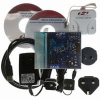
DEV KIT F220/221/226/230/231/236
Manufacturer
Silicon Laboratories Inc
Type
MCUr
Datasheet
1.C8051F226DK.pdf
(146 pages)
Specifications of C8051F226DK
Contents
Evaluation Board, Power Supply, USB Cables, Adapter and Documentation
Processor To Be Evaluated
C8051F22x and C8051F23x
Interface Type
USB
Silicon Manufacturer
Silicon Labs
Core Architecture
8051
Silicon Core Number
C8051F226
Silicon Family Name
C8051F2xx
Lead Free Status / RoHS Status
Contains lead / RoHS non-compliant
For Use With/related Products
C8051F220, 221, 226, 230, 231, 236
Lead Free Status / Rohs Status
Lead free / RoHS Compliant
Other names
336-1241


18. JTAG
Description
The MCU has an on-chip JTAG interface and logic to support Flash read and write operations and non-
intrusive in-circuit debug. The C8051F2xx may be placed in a JTAG test chain in order to maintain only
one JTAG interface in a system for boundary scan of other parts, and still utilize the C8051F2xx debug and
Flash programming. However, the C8051F2xx does NOT support boundary scan and will act as BYPASS
as specified in IEEE 1149.1.
The JTAG interface is implemented via four dedicated pins on the MCU, which are TCK, TMS, TDI, and
TDO. These pins are all 5 volt tolerant.
Through the 16-bit JTAG Instruction Register (IR), five instructions shown in JTAG Register Definition 18.1
can be commanded. These commands can either select the device ID code, or select registers for Flash
programming operations. BYPASS is shown to illustrate its default setting. There are four Data Registers
associated with the Flash read and write operations on the MCU.
Bit15
IR value
0xFFFF
0x0004
0x0082
0x0083
0x0084
0x0085
Flash Address
Flash Control
Instruction
Flash Scale
Flash Data
BYPASS
IDCODE
JTAG Register Definition 18.1. IR: JTAG Instruction
Selects device ID Register
Selects bypass Data Register and is DEFAULT for the device. Note:
The device does NOT support boundary scan. However, it may be
placed in a scan chain and bypassed in a system of other devices utiliz-
ing boundary scan.
Selects FLASHCON Register to control how the interface logic
responds to reads and writes to the FLASHDAT Register
Selects FLASHDAT Register for reads and writes to the Flash memory
Selects FLASHADR Register which holds the address of all Flash read,
write, and erase operations
Selects FLASHSCL Register which controls the prescaler used to gen-
erate timing signals for Flash operations
Rev. 1.6
Description
C8051F2xx
Bit0
Reset Value
0x0000
139
Related parts for C8051F226DK
Image
Part Number
Description
Manufacturer
Datasheet
Request
R

Part Number:
Description:
SMD/C°/SINGLE-ENDED OUTPUT SILICON OSCILLATOR
Manufacturer:
Silicon Laboratories Inc
Part Number:
Description:
Manufacturer:
Silicon Laboratories Inc
Datasheet:
Part Number:
Description:
N/A N/A/SI4010 AES KEYFOB DEMO WITH LCD RX
Manufacturer:
Silicon Laboratories Inc
Datasheet:
Part Number:
Description:
N/A N/A/SI4010 SIMPLIFIED KEY FOB DEMO WITH LED RX
Manufacturer:
Silicon Laboratories Inc
Datasheet:
Part Number:
Description:
N/A/-40 TO 85 OC/EZLINK MODULE; F930/4432 HIGH BAND (REV E/B1)
Manufacturer:
Silicon Laboratories Inc
Part Number:
Description:
EZLink Module; F930/4432 Low Band (rev e/B1)
Manufacturer:
Silicon Laboratories Inc
Part Number:
Description:
I°/4460 10 DBM RADIO TEST CARD 434 MHZ
Manufacturer:
Silicon Laboratories Inc
Part Number:
Description:
I°/4461 14 DBM RADIO TEST CARD 868 MHZ
Manufacturer:
Silicon Laboratories Inc
Part Number:
Description:
I°/4463 20 DBM RFSWITCH RADIO TEST CARD 460 MHZ
Manufacturer:
Silicon Laboratories Inc
Part Number:
Description:
I°/4463 20 DBM RADIO TEST CARD 868 MHZ
Manufacturer:
Silicon Laboratories Inc
Part Number:
Description:
I°/4463 27 DBM RADIO TEST CARD 868 MHZ
Manufacturer:
Silicon Laboratories Inc
Part Number:
Description:
I°/4463 SKYWORKS 30 DBM RADIO TEST CARD 915 MHZ
Manufacturer:
Silicon Laboratories Inc
Part Number:
Description:
N/A N/A/-40 TO 85 OC/4463 RFMD 30 DBM RADIO TEST CARD 915 MHZ
Manufacturer:
Silicon Laboratories Inc
Part Number:
Description:
I°/4463 20 DBM RADIO TEST CARD 169 MHZ
Manufacturer:
Silicon Laboratories Inc