EVB9S08DZ60 Freescale Semiconductor, EVB9S08DZ60 Datasheet - Page 149
EVB9S08DZ60
Manufacturer Part Number
EVB9S08DZ60
Description
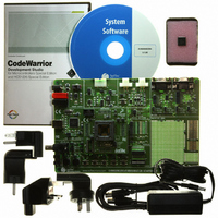
BOARD EVAL FOR 9S08DZ60
Manufacturer
Freescale Semiconductor
Type
MCUr
Datasheets
1.DEMO9S08DZ60.pdf
(416 pages)
2.EVB9S08DZ60.pdf
(2 pages)
3.EVB9S08DZ60.pdf
(32 pages)
4.EVB9S08DZ60.pdf
(13 pages)
5.EVB9S08DZ60.pdf
(4 pages)
Specifications of EVB9S08DZ60
Contents
Module and Misc Hardware
Processor To Be Evaluated
S08D
Data Bus Width
8 bit
Interface Type
RS-232, USB
Silicon Manufacturer
Freescale
Core Architecture
HCS08
Core Sub-architecture
HCS08
Silicon Core Number
MC9S08
Silicon Family Name
S08D
Kit Contents
Board Cables CD Power Supply
Rohs Compliant
Yes
For Use With/related Products
MC9S08DZ60
Lead Free Status / RoHS Status
Lead free / RoHS Compliant
Available stocks
Company
Part Number
Manufacturer
Quantity
Price
Company:

Part Number:
EVB9S08DZ60
Manufacturer:
TI
Quantity:
101


multiplication factor, as selected by the VDIV bits, times the reference frequency, as selected by the RDIV
bits. If BDM is enabled then the MCGLCLK is derived from the DCO (open-loop mode) divided by two.
If BDM is not enabled then the FLL is disabled in a low power state.
8.4.1.6
In PLL bypassed external (PBE) mode, the MCGOUT clock is derived from the external reference clock
and the PLL is operational but its output clock is not used. This mode is useful to allow the PLL to acquire
its target frequency while the MCGOUT clock is driven from the external reference clock.
The PLL bypassed external mode is entered when all the following conditions occur:
In PLL bypassed external mode, the MCGOUT clock is derived from the external reference clock. The
external reference clock which is enabled can be an external crystal/resonator or it can be another external
clock source. The PLL clock frequency locks to a multiplication factor, as selected by the VDIV bits, times
the reference frequency, as selected by the RDIV bits. If BDM is enabled then the MCGLCLK is derived
from the DCO (open-loop mode) divided by two. If BDM is not enabled then the FLL is disabled in a low
power state.
8.4.1.7
The bypassed low power internal (BLPI) mode is entered when all the following conditions occur:
In bypassed low power internal mode, the MCGOUT clock is derived from the internal reference clock.
The PLL and the FLL are disabled at all times in BLPI mode and the MCGLCLK will not be available for
BDC communications If the BDM becomes active the mode will switch to FLL bypassed internal (FBI)
mode.
8.4.1.8
The bypassed low power external (BLPE) mode is entered when all the following conditions occur:
Freescale Semiconductor
•
•
•
•
•
•
•
•
•
•
•
•
•
CLKS bits are written to 10
IREFS bit is written to 0
PLLS bit is written to 1
RDIV bits are written to divide reference clock to be within the range of 1 MHz to 2 MHz
LP bit is written to 0
CLKS bits are written to 01
IREFS bit is written to 1
PLLS bit is written to 0
LP bit is written to 1
BDM mode is not active
CLKS bits are written to 10
IREFS bit is written to 0
PLLS bit is written to 0 or 1
PLL Bypassed External (PBE)
Bypassed Low Power Internal (BLPI)
Bypassed Low Power External (BLPE)
MC9S08DZ60 Series Data Sheet, Rev. 4
Chapter 8 Multi-Purpose Clock Generator (S08MCGV1)
149
Related parts for EVB9S08DZ60
Image
Part Number
Description
Manufacturer
Datasheet
Request
R

Part Number:
Description:
Manufacturer:
Freescale Semiconductor, Inc
Datasheet:
Part Number:
Description:
Manufacturer:
Freescale Semiconductor, Inc
Datasheet:
Part Number:
Description:
Manufacturer:
Freescale Semiconductor, Inc
Datasheet:
Part Number:
Description:
Manufacturer:
Freescale Semiconductor, Inc
Datasheet:
Part Number:
Description:
Manufacturer:
Freescale Semiconductor, Inc
Datasheet:
Part Number:
Description:
Manufacturer:
Freescale Semiconductor, Inc
Datasheet:
Part Number:
Description:
Manufacturer:
Freescale Semiconductor, Inc
Datasheet:
Part Number:
Description:
Manufacturer:
Freescale Semiconductor, Inc
Datasheet:
Part Number:
Description:
Manufacturer:
Freescale Semiconductor, Inc
Datasheet:
Part Number:
Description:
Manufacturer:
Freescale Semiconductor, Inc
Datasheet:
Part Number:
Description:
Manufacturer:
Freescale Semiconductor, Inc
Datasheet:
Part Number:
Description:
Manufacturer:
Freescale Semiconductor, Inc
Datasheet:
Part Number:
Description:
Manufacturer:
Freescale Semiconductor, Inc
Datasheet:
Part Number:
Description:
Manufacturer:
Freescale Semiconductor, Inc
Datasheet:
Part Number:
Description:
Manufacturer:
Freescale Semiconductor, Inc
Datasheet: