EVB9S08DZ60 Freescale Semiconductor, EVB9S08DZ60 Datasheet - Page 188
EVB9S08DZ60
Manufacturer Part Number
EVB9S08DZ60
Description
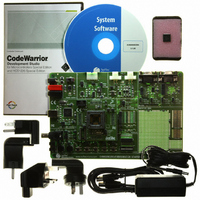
BOARD EVAL FOR 9S08DZ60
Manufacturer
Freescale Semiconductor
Type
MCUr
Datasheets
1.DEMO9S08DZ60.pdf
(416 pages)
2.EVB9S08DZ60.pdf
(2 pages)
3.EVB9S08DZ60.pdf
(32 pages)
4.EVB9S08DZ60.pdf
(13 pages)
5.EVB9S08DZ60.pdf
(4 pages)
Specifications of EVB9S08DZ60
Contents
Module and Misc Hardware
Processor To Be Evaluated
S08D
Data Bus Width
8 bit
Interface Type
RS-232, USB
Silicon Manufacturer
Freescale
Core Architecture
HCS08
Core Sub-architecture
HCS08
Silicon Core Number
MC9S08
Silicon Family Name
S08D
Kit Contents
Board Cables CD Power Supply
Rohs Compliant
Yes
For Use With/related Products
MC9S08DZ60
Lead Free Status / RoHS Status
Lead free / RoHS Compliant
Available stocks
Company
Part Number
Manufacturer
Quantity
Price
Company:

Part Number:
EVB9S08DZ60
Manufacturer:
TI
Quantity:
101


Chapter 10 Analog-to-Digital Converter (S08ADC12V1)
10.4.1
One of four clock sources can be selected as the clock source for the ADC module. This clock source is
then divided by a configurable value to generate the input clock to the converter (ADCK). The clock is
selected from one of the following sources by means of the ADICLK bits.
Whichever clock is selected, its frequency must fall within the specified frequency range for ADCK. If the
available clocks are too slow, the ADC do not perform according to specifications. If the available clocks
are too fast, the clock must be divided to the appropriate frequency. This divider is specified by the ADIV
bits and can be divide-by 1, 2, 4, or 8.
10.4.2
The pin control registers (APCTL3, APCTL2, and APCTL1) disable the I/O port control of the pins used
as analog inputs.When a pin control register bit is set, the following conditions are forced for the associated
MCU pin:
10.4.3
The ADC module has a selectable asynchronous hardware conversion trigger, ADHWT, that is enabled
when the ADTRG bit is set. This source is not available on all MCUs. Consult the module introduction for
information on the ADHWT source specific to this MCU.
When ADHWT source is available and hardware trigger is enabled (ADTRG=1), a conversion is initiated
on the rising edge of ADHWT. If a conversion is in progress when a rising edge occurs, the rising edge is
ignored. In continuous convert configuration, only the initial rising edge to launch continuous conversions
is observed. The hardware trigger function operates in conjunction with any of the conversion modes and
configurations.
10.4.4
Conversions can be performed in 12-bit mode, 10-bit mode, or 8-bit mode as determined by the MODE
bits. Conversions can be initiated by a software or hardware trigger. In addition, the ADC module can be
188
•
•
•
•
•
•
•
The bus clock, which is equal to the frequency at which software is executed. This is the default
selection following reset.
The bus clock divided by two. For higher bus clock rates, this allows a maximum divide by 16 of
the bus clock.
ALTCLK, as defined for this MCU (See module section introduction).
The asynchronous clock (ADACK). This clock is generated from a clock source within the ADC
module. When selected as the clock source, this clock remains active while the MCU is in wait or
stop3 mode and allows conversions in these modes for lower noise operation.
The output buffer is forced to its high impedance state.
The input buffer is disabled. A read of the I/O port returns a zero for any pin with its input buffer
disabled.
The pullup is disabled.
Clock Select and Divide Control
Input Select and Pin Control
Hardware Trigger
Conversion Control
MC9S08DZ60 Series Data Sheet, Rev. 4
Freescale Semiconductor
Related parts for EVB9S08DZ60
Image
Part Number
Description
Manufacturer
Datasheet
Request
R

Part Number:
Description:
Manufacturer:
Freescale Semiconductor, Inc
Datasheet:
Part Number:
Description:
Manufacturer:
Freescale Semiconductor, Inc
Datasheet:
Part Number:
Description:
Manufacturer:
Freescale Semiconductor, Inc
Datasheet:
Part Number:
Description:
Manufacturer:
Freescale Semiconductor, Inc
Datasheet:
Part Number:
Description:
Manufacturer:
Freescale Semiconductor, Inc
Datasheet:
Part Number:
Description:
Manufacturer:
Freescale Semiconductor, Inc
Datasheet:
Part Number:
Description:
Manufacturer:
Freescale Semiconductor, Inc
Datasheet:
Part Number:
Description:
Manufacturer:
Freescale Semiconductor, Inc
Datasheet:
Part Number:
Description:
Manufacturer:
Freescale Semiconductor, Inc
Datasheet:
Part Number:
Description:
Manufacturer:
Freescale Semiconductor, Inc
Datasheet:
Part Number:
Description:
Manufacturer:
Freescale Semiconductor, Inc
Datasheet:
Part Number:
Description:
Manufacturer:
Freescale Semiconductor, Inc
Datasheet:
Part Number:
Description:
Manufacturer:
Freescale Semiconductor, Inc
Datasheet:
Part Number:
Description:
Manufacturer:
Freescale Semiconductor, Inc
Datasheet:
Part Number:
Description:
Manufacturer:
Freescale Semiconductor, Inc
Datasheet: