EVB9S08DZ60 Freescale Semiconductor, EVB9S08DZ60 Datasheet - Page 154
EVB9S08DZ60
Manufacturer Part Number
EVB9S08DZ60
Description
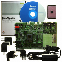
BOARD EVAL FOR 9S08DZ60
Manufacturer
Freescale Semiconductor
Type
MCUr
Datasheets
1.DEMO9S08DZ60.pdf
(416 pages)
2.EVB9S08DZ60.pdf
(2 pages)
3.EVB9S08DZ60.pdf
(32 pages)
4.EVB9S08DZ60.pdf
(13 pages)
5.EVB9S08DZ60.pdf
(4 pages)
Specifications of EVB9S08DZ60
Contents
Module and Misc Hardware
Processor To Be Evaluated
S08D
Data Bus Width
8 bit
Interface Type
RS-232, USB
Silicon Manufacturer
Freescale
Core Architecture
HCS08
Core Sub-architecture
HCS08
Silicon Core Number
MC9S08
Silicon Family Name
S08D
Kit Contents
Board Cables CD Power Supply
Rohs Compliant
Yes
For Use With/related Products
MC9S08DZ60
Lead Free Status / RoHS Status
Lead free / RoHS Compliant
Available stocks
Company
Part Number
Manufacturer
Quantity
Price
Company:

Part Number:
EVB9S08DZ60
Manufacturer:
TI
Quantity:
101


Chapter 8 Multi-Purpose Clock Generator (S08MCGV1)
The table below shows MCGOUT frequency calculations using RDIV, BDIV, and VDIV settings for each
clock mode. The bus frequency is equal to MCGOUT divided by 2.
This section will include 3 mode switching examples using a 4 MHz external crystal. If using an external
clock source less than 1 MHz, the MCG should not be configured for any of the PLL modes (PEE and
PBE).
8.5.2.1
In this example, the MCG will move through the proper operational modes from FEI to PEE mode until
the 4 MHz crystal reference frequency is set to achieve a bus frequency of 8 MHz. Because the MCG is in
FEI mode out of reset, this example also shows how to initialize the MCG for PEE mode out of reset. First,
the code sequence will be described. Then a flowchart will be included which illustrates the sequence.
154
1. First, FEI must transition to FBE mode:
1
FEI (FLL engaged internal)
FEE (FLL engaged external)
FBE (FLL bypassed external)
FBI (FLL bypassed internal)
PEE (PLL engaged external)
PBE (PLL bypassed external)
BLPI (Bypassed low power internal)
BLPE (Bypassed low power external)
a) MCGC2 = 0x36 (%00110110)
b) Loop until OSCINIT (bit 1) in MCGSC is 1, indicating the crystal selected by the EREFS bit
R is the reference divider selected by the RDIV bits, B is the bus frequency divider selected by the BDIV bits,
and M is the multiplier selected by the VDIV bits.
– BDIV (bits 7 and 6) set to %00, or divide-by-1
– RANGE (bit 5) set to 1 because the frequency of 4 MHz is within the high frequency range
– HGO (bit 4) set to 1 to configure external oscillator for high gain operation
– EREFS (bit 2) set to 1, because a crystal is being used
– ERCLKEN (bit 1) set to 1 to ensure the external reference clock is active
has been initialized.
Example # 1: Moving from FEI to PEE Mode: External Crystal = 4 MHz,
Bus Frequency = 8 MHz
Clock Mode
Table 8-6. MCGOUT Frequency Calculation Options
MC9S08DZ60 Series Data Sheet, Rev. 4
(f
(f
f
f
[(f
f
f
f
ext
int
ext
int
ext
int
ext
ext
/ B
/ B
/ B
/ B
/ B
* 1024) / B
/ R *1024) / B
/ R) * M] / B
f
MCGOUT
1
Typical f
immediately after reset. RDIV
bits set to %000.
f
31.25 kHz to 39.0625 kHz
f
31.25 kHz to 39.0625 kHz
Typical f
f
MHz to 2 MHz
f
MHz to 2 MHz
ext
ext
ext
ext
/ R must be in the range of
/ R must be in the range of
/ R must be in the range of 1
/ R must be in the range of 1
MCGOUT
int
= 32 kHz
Note
Freescale Semiconductor
= 16 MHz
Related parts for EVB9S08DZ60
Image
Part Number
Description
Manufacturer
Datasheet
Request
R

Part Number:
Description:
Manufacturer:
Freescale Semiconductor, Inc
Datasheet:
Part Number:
Description:
Manufacturer:
Freescale Semiconductor, Inc
Datasheet:
Part Number:
Description:
Manufacturer:
Freescale Semiconductor, Inc
Datasheet:
Part Number:
Description:
Manufacturer:
Freescale Semiconductor, Inc
Datasheet:
Part Number:
Description:
Manufacturer:
Freescale Semiconductor, Inc
Datasheet:
Part Number:
Description:
Manufacturer:
Freescale Semiconductor, Inc
Datasheet:
Part Number:
Description:
Manufacturer:
Freescale Semiconductor, Inc
Datasheet:
Part Number:
Description:
Manufacturer:
Freescale Semiconductor, Inc
Datasheet:
Part Number:
Description:
Manufacturer:
Freescale Semiconductor, Inc
Datasheet:
Part Number:
Description:
Manufacturer:
Freescale Semiconductor, Inc
Datasheet:
Part Number:
Description:
Manufacturer:
Freescale Semiconductor, Inc
Datasheet:
Part Number:
Description:
Manufacturer:
Freescale Semiconductor, Inc
Datasheet:
Part Number:
Description:
Manufacturer:
Freescale Semiconductor, Inc
Datasheet:
Part Number:
Description:
Manufacturer:
Freescale Semiconductor, Inc
Datasheet:
Part Number:
Description:
Manufacturer:
Freescale Semiconductor, Inc
Datasheet: