EVB9S08DZ60 Freescale Semiconductor, EVB9S08DZ60 Datasheet - Page 150
EVB9S08DZ60
Manufacturer Part Number
EVB9S08DZ60
Description
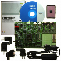
BOARD EVAL FOR 9S08DZ60
Manufacturer
Freescale Semiconductor
Type
MCUr
Datasheets
1.DEMO9S08DZ60.pdf
(416 pages)
2.EVB9S08DZ60.pdf
(2 pages)
3.EVB9S08DZ60.pdf
(32 pages)
4.EVB9S08DZ60.pdf
(13 pages)
5.EVB9S08DZ60.pdf
(4 pages)
Specifications of EVB9S08DZ60
Contents
Module and Misc Hardware
Processor To Be Evaluated
S08D
Data Bus Width
8 bit
Interface Type
RS-232, USB
Silicon Manufacturer
Freescale
Core Architecture
HCS08
Core Sub-architecture
HCS08
Silicon Core Number
MC9S08
Silicon Family Name
S08D
Kit Contents
Board Cables CD Power Supply
Rohs Compliant
Yes
For Use With/related Products
MC9S08DZ60
Lead Free Status / RoHS Status
Lead free / RoHS Compliant
Available stocks
Company
Part Number
Manufacturer
Quantity
Price
Company:

Part Number:
EVB9S08DZ60
Manufacturer:
TI
Quantity:
101


Chapter 8 Multi-Purpose Clock Generator (S08MCGV1)
In bypassed low power external mode, the MCGOUT clock is derived from the external reference clock.
The external reference clock which is enabled can be an external crystal/resonator or it can be another
external clock source.
The PLL and the FLL are disabled at all times in BLPE mode and the MCGLCLK will not be available
for BDC communications. If the BDM becomes active the mode will switch to one of the bypassed
external modes as determined by the state of the PLLS bit.
8.4.1.9
Stop mode is entered whenever the MCU enters a STOP state. In this mode, the FLL and PLL are disabled
and all MCG clock signals are static except in the following cases:
MCGIRCLK will be active in stop mode when all the following conditions occur:
MCGERCLK will be active in stop mode when all the following conditions occur:
8.4.2
When switching between engaged internal and engaged external modes the IREFS bit can be changed at
anytime, but the RDIV bits must be changed simultaneously so that the reference frequency stays in the
range required by the state of the PLLS bit (31.25 kHz to 39.0625 kHz if the FLL is selected, or 1 MHz to
2 MHz if the PLL is selected). After a change in the IREFS value the FLL or PLL will begin locking again
after the switch is completed. The completion of the switch is shown by the IREFST bit .
For the special case of entering stop mode immediately after switching to FBE mode, if the external clock
and the internal clock are disabled in stop mode, (EREFSTEN = 0 and IREFSTEN = 0), it is necessary to
allow 100us after the IREFST bit is cleared to allow the internal reference to shutdown. For most cases the
delay due to instruction execution times will be sufficient.
The CLKS bits can also be changed at anytime, but in order for the MCGLCLK to be configured correctly
the RDIV bits must be changed simultaneously so that the reference frequency stays in the range required
by the state of the PLLS bit (31.25 kHz to 39.0625 kHz if the FLL is selected, or 1 MHz to 2MHz if the
PLL is selected). The actual switch to the newly selected clock will be shown by the CLKST bits. If the
newly selected clock is not available, the previous clock will remain selected.
For details see
150
•
•
•
•
•
•
LP bit is written to 1
BDM mode is not active
IRCLKEN = 1
IREFSTEN = 1
ERCLKEN = 1
EREFSTEN = 1
Mode Switching
Stop
Figure
8-8.
MC9S08DZ60 Series Data Sheet, Rev. 4
Freescale Semiconductor
Related parts for EVB9S08DZ60
Image
Part Number
Description
Manufacturer
Datasheet
Request
R

Part Number:
Description:
Manufacturer:
Freescale Semiconductor, Inc
Datasheet:
Part Number:
Description:
Manufacturer:
Freescale Semiconductor, Inc
Datasheet:
Part Number:
Description:
Manufacturer:
Freescale Semiconductor, Inc
Datasheet:
Part Number:
Description:
Manufacturer:
Freescale Semiconductor, Inc
Datasheet:
Part Number:
Description:
Manufacturer:
Freescale Semiconductor, Inc
Datasheet:
Part Number:
Description:
Manufacturer:
Freescale Semiconductor, Inc
Datasheet:
Part Number:
Description:
Manufacturer:
Freescale Semiconductor, Inc
Datasheet:
Part Number:
Description:
Manufacturer:
Freescale Semiconductor, Inc
Datasheet:
Part Number:
Description:
Manufacturer:
Freescale Semiconductor, Inc
Datasheet:
Part Number:
Description:
Manufacturer:
Freescale Semiconductor, Inc
Datasheet:
Part Number:
Description:
Manufacturer:
Freescale Semiconductor, Inc
Datasheet:
Part Number:
Description:
Manufacturer:
Freescale Semiconductor, Inc
Datasheet:
Part Number:
Description:
Manufacturer:
Freescale Semiconductor, Inc
Datasheet:
Part Number:
Description:
Manufacturer:
Freescale Semiconductor, Inc
Datasheet:
Part Number:
Description:
Manufacturer:
Freescale Semiconductor, Inc
Datasheet: