EVB9S08DZ60 Freescale Semiconductor, EVB9S08DZ60 Datasheet - Page 53
EVB9S08DZ60
Manufacturer Part Number
EVB9S08DZ60
Description
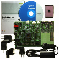
BOARD EVAL FOR 9S08DZ60
Manufacturer
Freescale Semiconductor
Type
MCUr
Datasheets
1.DEMO9S08DZ60.pdf
(416 pages)
2.EVB9S08DZ60.pdf
(2 pages)
3.EVB9S08DZ60.pdf
(32 pages)
4.EVB9S08DZ60.pdf
(13 pages)
5.EVB9S08DZ60.pdf
(4 pages)
Specifications of EVB9S08DZ60
Contents
Module and Misc Hardware
Processor To Be Evaluated
S08D
Data Bus Width
8 bit
Interface Type
RS-232, USB
Silicon Manufacturer
Freescale
Core Architecture
HCS08
Core Sub-architecture
HCS08
Silicon Core Number
MC9S08
Silicon Family Name
S08D
Kit Contents
Board Cables CD Power Supply
Rohs Compliant
Yes
For Use With/related Products
MC9S08DZ60
Lead Free Status / RoHS Status
Lead free / RoHS Compliant
Available stocks
Company
Part Number
Manufacturer
Quantity
Price
Company:

Part Number:
EVB9S08DZ60
Manufacturer:
TI
Quantity:
101


4.5.2
Before any program or erase command can be accepted, the Flash and EEPROM clock divider register
(FCDIV) must be written to set the internal clock for the Flash and EEPROM module to a frequency
(f
Register
reset initialization. The user must ensure that FACCERR is not set before writing to the FCDIV register.
One period of the resulting clock (1/f
pulses. An integer number of these timing pulses is used by the command processor to complete a program
or erase command.
Table 4-6
of FCLK (f
of cycles of FCLK and as an absolute time for the case where t
shown include overhead for the command state machine and enabling and disabling of program and erase
voltages.
4.5.3
The FCDIV register must be initialized after any reset and any error flag is cleared before beginning
command execution. The command execution steps are:
Freescale Semiconductor
FCLK
•
•
1. Write a data value to an address in the Flash or EEPROM array. The address and data information
) between 150 kHz and 200 kHz (see
Burst programming capability
Sector erase abort
from this write is latched into the Flash and EEPROM interface. This write is a required first step
in any command sequence. For erase and blank check commands, the value of the data is not
important. For sector erase commands, the address can be any address in the sector of Flash or
EEPROM to be erased. For mass erase and blank check commands, the address can be any address
in the Flash or EEPROM memory. Flash and EEPROM erase independently of each other.
(FCDIV)”). This register can be written only once, so normally this write is performed during
shows program and erase times. The bus clock frequency and FCDIV determine the frequency
FCLK
Program and Erase Times
Program and Erase Command Execution
1
Excluding start/end overhead
). The time for one cycle of FCLK is t
Sector erase abort
Burst program
Byte program
Sector erase
Mass erase
Parameter
Table 4-6. Program and Erase Times
MC9S08DZ60 Series Data Sheet, Rev. 4
FCLK
) is used by the command processor to time program and erase
Section 4.5.11.1, “Flash and EEPROM Clock Divider
Cycles of FCLK
20,000
4000
9
4
4
FCLK
= 1/f
FCLK
FCLK
Time if FCLK = 200 kHz
= 5 μs. Program and erase times
. The times are shown as a number
100 ms
20 μs
20 μs
20 ms
45 μs
1
1
Chapter 4 Memory
53
Related parts for EVB9S08DZ60
Image
Part Number
Description
Manufacturer
Datasheet
Request
R

Part Number:
Description:
Manufacturer:
Freescale Semiconductor, Inc
Datasheet:
Part Number:
Description:
Manufacturer:
Freescale Semiconductor, Inc
Datasheet:
Part Number:
Description:
Manufacturer:
Freescale Semiconductor, Inc
Datasheet:
Part Number:
Description:
Manufacturer:
Freescale Semiconductor, Inc
Datasheet:
Part Number:
Description:
Manufacturer:
Freescale Semiconductor, Inc
Datasheet:
Part Number:
Description:
Manufacturer:
Freescale Semiconductor, Inc
Datasheet:
Part Number:
Description:
Manufacturer:
Freescale Semiconductor, Inc
Datasheet:
Part Number:
Description:
Manufacturer:
Freescale Semiconductor, Inc
Datasheet:
Part Number:
Description:
Manufacturer:
Freescale Semiconductor, Inc
Datasheet:
Part Number:
Description:
Manufacturer:
Freescale Semiconductor, Inc
Datasheet:
Part Number:
Description:
Manufacturer:
Freescale Semiconductor, Inc
Datasheet:
Part Number:
Description:
Manufacturer:
Freescale Semiconductor, Inc
Datasheet:
Part Number:
Description:
Manufacturer:
Freescale Semiconductor, Inc
Datasheet:
Part Number:
Description:
Manufacturer:
Freescale Semiconductor, Inc
Datasheet:
Part Number:
Description:
Manufacturer:
Freescale Semiconductor, Inc
Datasheet: