EVB9S08DZ60 Freescale Semiconductor, EVB9S08DZ60 Datasheet - Page 350
EVB9S08DZ60
Manufacturer Part Number
EVB9S08DZ60
Description
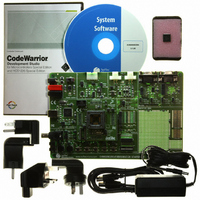
BOARD EVAL FOR 9S08DZ60
Manufacturer
Freescale Semiconductor
Type
MCUr
Datasheets
1.DEMO9S08DZ60.pdf
(416 pages)
2.EVB9S08DZ60.pdf
(2 pages)
3.EVB9S08DZ60.pdf
(32 pages)
4.EVB9S08DZ60.pdf
(13 pages)
5.EVB9S08DZ60.pdf
(4 pages)
Specifications of EVB9S08DZ60
Contents
Module and Misc Hardware
Processor To Be Evaluated
S08D
Data Bus Width
8 bit
Interface Type
RS-232, USB
Silicon Manufacturer
Freescale
Core Architecture
HCS08
Core Sub-architecture
HCS08
Silicon Core Number
MC9S08
Silicon Family Name
S08D
Kit Contents
Board Cables CD Power Supply
Rohs Compliant
Yes
For Use With/related Products
MC9S08DZ60
Lead Free Status / RoHS Status
Lead free / RoHS Compliant
Available stocks
Company
Part Number
Manufacturer
Quantity
Price
Company:

Part Number:
EVB9S08DZ60
Manufacturer:
TI
Quantity:
101


Chapter 17 Development Support
When no debugger pod is connected to the 6-pin BDM interface connector, the internal pullup on BKGD
chooses normal operating mode. When a debug pod is connected to BKGD it is possible to force the MCU
into active background mode after reset. The specific conditions for forcing active background depend
upon the HCS08 derivative (refer to the introduction to this Development Support section). It is not
necessary to reset the target MCU to communicate with it through the background debug interface.
17.2.2
Communication Details
The BDC serial interface requires the external controller to generate a falling edge on the BKGD pin to
indicate the start of each bit time. The external controller provides this falling edge whether data is
transmitted or received.
BKGD is a pseudo-open-drain pin that can be driven either by an external controller or by the MCU. Data
is transferred MSB first at 16 BDC clock cycles per bit (nominal speed). The interface times out if
512 BDC clock cycles occur between falling edges from the host. Any BDC command that was in progress
when this timeout occurs is aborted without affecting the memory or operating mode of the target MCU
system.
The custom serial protocol requires the debug pod to know the target BDC communication clock speed.
The clock switch (CLKSW) control bit in the BDC status and control register allows the user to select the
BDC clock source. The BDC clock source can either be the bus or the alternate BDC clock source.
The BKGD pin can receive a high or low level or transmit a high or low level. The following diagrams
show timing for each of these cases. Interface timing is synchronous to clocks in the target BDC, but
asynchronous to the external host. The internal BDC clock signal is shown for reference in counting cycles.
MC9S08DZ60 Series Data Sheet, Rev. 4
350
Freescale Semiconductor
Related parts for EVB9S08DZ60
Image
Part Number
Description
Manufacturer
Datasheet
Request
R

Part Number:
Description:
Manufacturer:
Freescale Semiconductor, Inc
Datasheet:
Part Number:
Description:
Manufacturer:
Freescale Semiconductor, Inc
Datasheet:
Part Number:
Description:
Manufacturer:
Freescale Semiconductor, Inc
Datasheet:
Part Number:
Description:
Manufacturer:
Freescale Semiconductor, Inc
Datasheet:
Part Number:
Description:
Manufacturer:
Freescale Semiconductor, Inc
Datasheet:
Part Number:
Description:
Manufacturer:
Freescale Semiconductor, Inc
Datasheet:
Part Number:
Description:
Manufacturer:
Freescale Semiconductor, Inc
Datasheet:
Part Number:
Description:
Manufacturer:
Freescale Semiconductor, Inc
Datasheet:
Part Number:
Description:
Manufacturer:
Freescale Semiconductor, Inc
Datasheet:
Part Number:
Description:
Manufacturer:
Freescale Semiconductor, Inc
Datasheet:
Part Number:
Description:
Manufacturer:
Freescale Semiconductor, Inc
Datasheet:
Part Number:
Description:
Manufacturer:
Freescale Semiconductor, Inc
Datasheet:
Part Number:
Description:
Manufacturer:
Freescale Semiconductor, Inc
Datasheet:
Part Number:
Description:
Manufacturer:
Freescale Semiconductor, Inc
Datasheet:
Part Number:
Description:
Manufacturer:
Freescale Semiconductor, Inc
Datasheet: