EVB9S08DZ60 Freescale Semiconductor, EVB9S08DZ60 Datasheet - Page 210
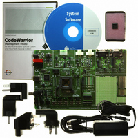
EVB9S08DZ60
Manufacturer Part Number
EVB9S08DZ60
Description
BOARD EVAL FOR 9S08DZ60
Manufacturer
Freescale Semiconductor
Type
MCUr
Datasheets
1.DEMO9S08DZ60.pdf
(416 pages)
2.EVB9S08DZ60.pdf
(2 pages)
3.EVB9S08DZ60.pdf
(32 pages)
4.EVB9S08DZ60.pdf
(13 pages)
5.EVB9S08DZ60.pdf
(4 pages)
Specifications of EVB9S08DZ60
Contents
Module and Misc Hardware
Processor To Be Evaluated
S08D
Data Bus Width
8 bit
Interface Type
RS-232, USB
Silicon Manufacturer
Freescale
Core Architecture
HCS08
Core Sub-architecture
HCS08
Silicon Core Number
MC9S08
Silicon Family Name
S08D
Kit Contents
Board Cables CD Power Supply
Rohs Compliant
Yes
For Use With/related Products
MC9S08DZ60
Lead Free Status / RoHS Status
Lead free / RoHS Compliant
Available stocks
Company
Part Number
Manufacturer
Quantity
Price
Company:

Part Number:
EVB9S08DZ60
Manufacturer:
TI
Quantity:
101


Chapter 11 Inter-Integrated Circuit (S08IICV2)
11.4.1.1
When the bus is free, no master device is engaging the bus (SCL and SDA lines are at logical high), a
master may initiate communication by sending a start signal. As shown in
defined as a high-to-low transition of SDA while SCL is high. This signal denotes the beginning of a new
data transfer (each data transfer may contain several bytes of data) and brings all slaves out of their idle
states.
11.4.1.2
The first byte of data transferred immediately after the start signal is the slave address transmitted by the
master. This is a seven-bit calling address followed by a R/W bit. The R/W bit tells the slave the desired
direction of data transfer.
Only the slave with a calling address that matches the one transmitted by the master responds by sending
back an acknowledge bit. This is done by pulling the SDA low at the ninth clock (see
No two slaves in the system may have the same address. If the IIC module is the master, it must not transmit
an address equal to its own slave address. The IIC cannot be master and slave at the same time. However,
if arbitration is lost during an address cycle, the IIC reverts to slave mode and operates correctly even if it
is being addressed by another master.
210
1 = Read transfer, the slave transmits data to the master.
0 = Write transfer, the master transmits data to the slave.
SCL
SDA
SCL
SDA
Signal
Signal
Start
Start
Start Signal
Slave Address Transmission
msb
AD7 AD6 AD5 AD4 AD3 AD2 AD1 R/W
msb
AD7 AD6 AD5 AD4 AD3 AD2 AD1 R/W
1
1
2
2
Calling Address
Calling Address
3
3
4
4
5
5
Figure 11-9. IIC Bus Transmission Signals
MC9S08DZ60 Series Data Sheet, Rev. 4
6
6
7
7
Read/
Read/
Write
Write
lsb
lsb
8
8
Ack
Ack
Bit
Bit
9
9
XX
Repeated
XXX
Signal
Start
msb
msb
AD7 AD6 AD5 AD4 AD3 AD2 AD1 R/W
D7
1
1
D6
2
2
New Calling Address
D5
3
3
Data Byte
D4
4
4
D3
Figure
5
5
D2
6
6
11-9, a start signal is
D1
7
7
Freescale Semiconductor
Read/
Write
Figure
lsb
lsb
D0
8
8
Ack
No
Bit
Ack
No
9
Bit
9
11-9).
Signal
Stop
Signal
Stop
Related parts for EVB9S08DZ60
Image
Part Number
Description
Manufacturer
Datasheet
Request
R

Part Number:
Description:
Manufacturer:
Freescale Semiconductor, Inc
Datasheet:
Part Number:
Description:
Manufacturer:
Freescale Semiconductor, Inc
Datasheet:
Part Number:
Description:
Manufacturer:
Freescale Semiconductor, Inc
Datasheet:
Part Number:
Description:
Manufacturer:
Freescale Semiconductor, Inc
Datasheet:
Part Number:
Description:
Manufacturer:
Freescale Semiconductor, Inc
Datasheet:
Part Number:
Description:
Manufacturer:
Freescale Semiconductor, Inc
Datasheet:
Part Number:
Description:
Manufacturer:
Freescale Semiconductor, Inc
Datasheet:
Part Number:
Description:
Manufacturer:
Freescale Semiconductor, Inc
Datasheet:
Part Number:
Description:
Manufacturer:
Freescale Semiconductor, Inc
Datasheet:
Part Number:
Description:
Manufacturer:
Freescale Semiconductor, Inc
Datasheet:
Part Number:
Description:
Manufacturer:
Freescale Semiconductor, Inc
Datasheet:
Part Number:
Description:
Manufacturer:
Freescale Semiconductor, Inc
Datasheet:
Part Number:
Description:
Manufacturer:
Freescale Semiconductor, Inc
Datasheet:
Part Number:
Description:
Manufacturer:
Freescale Semiconductor, Inc
Datasheet:
Part Number:
Description:
Manufacturer:
Freescale Semiconductor, Inc
Datasheet: