EVB9S08DZ60 Freescale Semiconductor, EVB9S08DZ60 Datasheet - Page 295
EVB9S08DZ60
Manufacturer Part Number
EVB9S08DZ60
Description
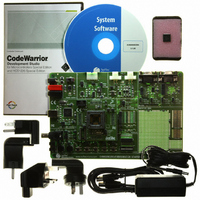
BOARD EVAL FOR 9S08DZ60
Manufacturer
Freescale Semiconductor
Type
MCUr
Datasheets
1.DEMO9S08DZ60.pdf
(416 pages)
2.EVB9S08DZ60.pdf
(2 pages)
3.EVB9S08DZ60.pdf
(32 pages)
4.EVB9S08DZ60.pdf
(13 pages)
5.EVB9S08DZ60.pdf
(4 pages)
Specifications of EVB9S08DZ60
Contents
Module and Misc Hardware
Processor To Be Evaluated
S08D
Data Bus Width
8 bit
Interface Type
RS-232, USB
Silicon Manufacturer
Freescale
Core Architecture
HCS08
Core Sub-architecture
HCS08
Silicon Core Number
MC9S08
Silicon Family Name
S08D
Kit Contents
Board Cables CD Power Supply
Rohs Compliant
Yes
For Use With/related Products
MC9S08DZ60
Lead Free Status / RoHS Status
Lead free / RoHS Compliant
Available stocks
Company
Part Number
Manufacturer
Quantity
Price
Company:

Part Number:
EVB9S08DZ60
Manufacturer:
TI
Quantity:
101


14.2.2
This read/write register is used to control various optional features of the SCI system.
Freescale Semiconductor
SCISWAI
SBR[7:0]
Reset
Reset
LOOPS
RSRC
Field
Field
7:0
M
7
6
5
4
W
W
R
R
LOOPS
SBR7
SCI Control Register 1 (SCIxC1)
Baud Rate Modulo Divisor — These 13 bits in SBR[12:0] are referred to collectively as BR, and they set the
modulo divide rate for the SCI baud rate generator. When BR = 0, the SCI baud rate generator is disabled to
reduce supply current. When BR = 1 to 8191, the SCI baud rate = BUSCLK/(16×BR). See also BR bits in
Table
Loop Mode Select — Selects between loop back modes and normal 2-pin full-duplex modes. When
LOOPS = 1, the transmitter output is internally connected to the receiver input.
0 Normal operation — RxD and TxD use separate pins.
1 Loop mode or single-wire mode where transmitter outputs are internally connected to receiver input. (See
SCI Stops in Wait Mode
0 SCI clocks continue to run in wait mode so the SCI can be the source of an interrupt that wakes up the CPU.
1 SCI clocks freeze while CPU is in wait mode.
Receiver Source Select — This bit has no meaning or effect unless the LOOPS bit is set to 1. When
LOOPS = 1, the receiver input is internally connected to the TxD pin and RSRC determines whether this
connection is also connected to the transmitter output.
0 Provided LOOPS = 1, RSRC = 0 selects internal loop back mode and the SCI does not use the RxD pins.
1 Single-wire SCI mode where the TxD pin is connected to the transmitter output and receiver input.
9-Bit or 8-Bit Mode Select
0 Normal — start + 8 data bits (LSB first) + stop.
1 Receiver and transmitter use 9-bit data characters
0
0
7
7
RSRC
start + 8 data bits (LSB first) + 9th data bit + stop.
14-2.
bit.) RxD pin is not used by SCI.
SCISWAI
SBR6
0
0
6
6
Figure 14-5. SCI Baud Rate Register (SCIxBDL)
Figure 14-6. SCI Control Register 1 (SCIxC1)
Table 14-3. SCIxBDL Field Descriptions
Table 14-4. SCIxC1 Field Descriptions
MC9S08DZ60 Series Data Sheet, Rev. 4
RSRC
SBR5
0
0
5
5
SBR4
M
0
0
4
4
Description
Description
WAKE
SBR3
Chapter 14 Serial Communications Interface (S08SCIV4)
3
0
3
0
SBR2
ILT
1
0
2
2
SBR1
PE
0
0
1
1
SBR0
PT
0
0
0
0
295
Related parts for EVB9S08DZ60
Image
Part Number
Description
Manufacturer
Datasheet
Request
R

Part Number:
Description:
Manufacturer:
Freescale Semiconductor, Inc
Datasheet:
Part Number:
Description:
Manufacturer:
Freescale Semiconductor, Inc
Datasheet:
Part Number:
Description:
Manufacturer:
Freescale Semiconductor, Inc
Datasheet:
Part Number:
Description:
Manufacturer:
Freescale Semiconductor, Inc
Datasheet:
Part Number:
Description:
Manufacturer:
Freescale Semiconductor, Inc
Datasheet:
Part Number:
Description:
Manufacturer:
Freescale Semiconductor, Inc
Datasheet:
Part Number:
Description:
Manufacturer:
Freescale Semiconductor, Inc
Datasheet:
Part Number:
Description:
Manufacturer:
Freescale Semiconductor, Inc
Datasheet:
Part Number:
Description:
Manufacturer:
Freescale Semiconductor, Inc
Datasheet:
Part Number:
Description:
Manufacturer:
Freescale Semiconductor, Inc
Datasheet:
Part Number:
Description:
Manufacturer:
Freescale Semiconductor, Inc
Datasheet:
Part Number:
Description:
Manufacturer:
Freescale Semiconductor, Inc
Datasheet:
Part Number:
Description:
Manufacturer:
Freescale Semiconductor, Inc
Datasheet:
Part Number:
Description:
Manufacturer:
Freescale Semiconductor, Inc
Datasheet:
Part Number:
Description:
Manufacturer:
Freescale Semiconductor, Inc
Datasheet: