EVB9S08DZ60 Freescale Semiconductor, EVB9S08DZ60 Datasheet - Page 155
EVB9S08DZ60
Manufacturer Part Number
EVB9S08DZ60
Description
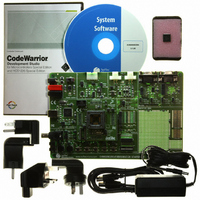
BOARD EVAL FOR 9S08DZ60
Manufacturer
Freescale Semiconductor
Type
MCUr
Datasheets
1.DEMO9S08DZ60.pdf
(416 pages)
2.EVB9S08DZ60.pdf
(2 pages)
3.EVB9S08DZ60.pdf
(32 pages)
4.EVB9S08DZ60.pdf
(13 pages)
5.EVB9S08DZ60.pdf
(4 pages)
Specifications of EVB9S08DZ60
Contents
Module and Misc Hardware
Processor To Be Evaluated
S08D
Data Bus Width
8 bit
Interface Type
RS-232, USB
Silicon Manufacturer
Freescale
Core Architecture
HCS08
Core Sub-architecture
HCS08
Silicon Core Number
MC9S08
Silicon Family Name
S08D
Kit Contents
Board Cables CD Power Supply
Rohs Compliant
Yes
For Use With/related Products
MC9S08DZ60
Lead Free Status / RoHS Status
Lead free / RoHS Compliant
Available stocks
Company
Part Number
Manufacturer
Quantity
Price
Company:

Part Number:
EVB9S08DZ60
Manufacturer:
TI
Quantity:
101


Freescale Semiconductor
2. Then, FBE must transition either directly to PBE mode or first through BLPE mode and then to
3. Last, PBE mode transitions into PEE mode:
c) MCGC1 = 0xB8 (%10111000)
d) Loop until IREFST (bit 4) in MCGSC is 0, indicating the external reference is the current
e) Loop until CLKST (bits 3 and 2) in MCGSC are %10, indicating that the external reference
PBE mode:
a) BLPE: If a transition through BLPE mode is desired, first set LP (bit 3) in MCGC2 to 1.
b) BLPE/PBE: MCGC1 = 0x90 (%10010000)
c) BLPE/PBE: MCGC3 = 0x44 (%01000100)
d) BLPE: If transitioning through BLPE mode, clear LP (bit 3) in MCGC2 to 0 here to switch to
e) PBE: Loop until PLLST (bit 5) in MCGSC is set, indicating that the current source for the
f) PBE: Then loop until LOCK (bit 6) in MCGSC is set, indicating that the PLL has acquired lock
a) MCGC1 = 0x10 (%00010000)
b) Loop until CLKST (bits 3 and 2) in MCGSC are %11, indicating that the PLL output is selected
– CLKS (bits 7 and 6) set to %10 in order to select external reference clock as system clock
– RDIV (bits 5-3) set to %111, or divide-by-128 because 4 MHz / 128 = 31.25 kHz which is
– IREFS (bit 2) cleared to 0, selecting the external reference clock
source for the reference clock
clock is selected to feed MCGOUT
– RDIV (bits 5-3) set to %010, or divide-by-4 because 4 MHz / 4 = 1 MHz which is in the 1
– PLLS (bit 6) set to 1, selects the PLL. In BLPE mode, changing this bit only prepares the
– VDIV (bits 3-0) set to %0100, or multiply-by-16 because 1 MHz reference * 16 = 16 MHz.
PBE mode
PLLS clock is the PLL
– CLKS (bits7 and 6) in MCGSC1 set to %00 in order to select the output of the PLL as the
to feed MCGOUT in the current clock mode
– Now, With an RDIV of divide-by-4, a BDIV of divide-by-1, and a VDIV of multiply-by-16,
source
in the 31.25 kHz to 39.0625 kHz range required by the FLL
MHz to 2 MHz range required by the PLL. In BLPE mode, the configuration of the RDIV
does not matter because both the FLL and PLL are disabled. Changing them only sets up the
the dividers for PLL usage in PBE mode
MCG for PLL usage in PBE mode
In BLPE mode, the configuration of the VDIV bits does not matter because the PLL is
disabled. Changing them only sets up the multiply value for PLL usage in PBE mode
system clock source
MCGOUT = [(4 MHz / 4) * 16] / 1 = 16 MHz, and the bus frequency is MCGOUT / 2, or 8
MHz
MC9S08DZ60 Series Data Sheet, Rev. 4
Chapter 8 Multi-Purpose Clock Generator (S08MCGV1)
155
Related parts for EVB9S08DZ60
Image
Part Number
Description
Manufacturer
Datasheet
Request
R

Part Number:
Description:
Manufacturer:
Freescale Semiconductor, Inc
Datasheet:
Part Number:
Description:
Manufacturer:
Freescale Semiconductor, Inc
Datasheet:
Part Number:
Description:
Manufacturer:
Freescale Semiconductor, Inc
Datasheet:
Part Number:
Description:
Manufacturer:
Freescale Semiconductor, Inc
Datasheet:
Part Number:
Description:
Manufacturer:
Freescale Semiconductor, Inc
Datasheet:
Part Number:
Description:
Manufacturer:
Freescale Semiconductor, Inc
Datasheet:
Part Number:
Description:
Manufacturer:
Freescale Semiconductor, Inc
Datasheet:
Part Number:
Description:
Manufacturer:
Freescale Semiconductor, Inc
Datasheet:
Part Number:
Description:
Manufacturer:
Freescale Semiconductor, Inc
Datasheet:
Part Number:
Description:
Manufacturer:
Freescale Semiconductor, Inc
Datasheet:
Part Number:
Description:
Manufacturer:
Freescale Semiconductor, Inc
Datasheet:
Part Number:
Description:
Manufacturer:
Freescale Semiconductor, Inc
Datasheet:
Part Number:
Description:
Manufacturer:
Freescale Semiconductor, Inc
Datasheet:
Part Number:
Description:
Manufacturer:
Freescale Semiconductor, Inc
Datasheet:
Part Number:
Description:
Manufacturer:
Freescale Semiconductor, Inc
Datasheet: