EVB9S08DZ60 Freescale Semiconductor, EVB9S08DZ60 Datasheet - Page 370
EVB9S08DZ60
Manufacturer Part Number
EVB9S08DZ60
Description
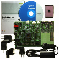
BOARD EVAL FOR 9S08DZ60
Manufacturer
Freescale Semiconductor
Type
MCUr
Datasheets
1.DEMO9S08DZ60.pdf
(416 pages)
2.EVB9S08DZ60.pdf
(2 pages)
3.EVB9S08DZ60.pdf
(32 pages)
4.EVB9S08DZ60.pdf
(13 pages)
5.EVB9S08DZ60.pdf
(4 pages)
Specifications of EVB9S08DZ60
Contents
Module and Misc Hardware
Processor To Be Evaluated
S08D
Data Bus Width
8 bit
Interface Type
RS-232, USB
Silicon Manufacturer
Freescale
Core Architecture
HCS08
Core Sub-architecture
HCS08
Silicon Core Number
MC9S08
Silicon Family Name
S08D
Kit Contents
Board Cables CD Power Supply
Rohs Compliant
Yes
For Use With/related Products
MC9S08DZ60
Lead Free Status / RoHS Status
Lead free / RoHS Compliant
Available stocks
Company
Part Number
Manufacturer
Quantity
Price
Company:

Part Number:
EVB9S08DZ60
Manufacturer:
TI
Quantity:
101


Appendix A Electrical Characteristics
This device contains circuitry protecting against damage due to high static voltage or electrical fields;
however, it is advised that normal precautions be taken to avoid application of any voltages higher than
maximum-rated voltages to this high-impedance circuit. Reliability of operation is enhanced if unused
inputs are tied to an appropriate logic voltage level (for instance, either V
A.4
This section provides information about operating temperature range, power dissipation, and package
thermal resistance. Power dissipation on I/O pins is usually small compared to the power dissipation in
on-chip logic and it is user-determined rather than being controlled by the MCU design. In order to take
P
V
loads), the difference between pin voltage and V
370
I/O
DD
into account in power calculations, determine the difference between actual pin voltage and V
and multiply by the pin current for each I/O pin. Except in cases of unusually high pin current (heavy
1
2
3
Thermal Characteristics
Num
Input must be current limited to the value specified. To determine the value of the required
current-limiting resistor, calculate resistance values for positive (V
voltages, then use the larger of the two resistance values.
All functional non-supply pins are internally clamped to V
Power supply must maintain regulation within operating V
maximum current conditions. If positive injection current (V
current may flow out of V
external V
risk when the MCU is not consuming power. Examples are: if no system clock is present, or if the clock
rate is very low which would reduce overall power consumption.
1
2
3
4
5
Supply voltage
Input voltage
Instantaneous maximum current
(applies to all port pins)
Maximum current into V
Storage temperature
DD
load will shunt current greater than maximum injection current. This will be the greatest
DD
Table A-2. Absolute Maximum Ratings
and could result in external power supply going out of regulation. Ensure
Rating
MC9S08DZ60 Series Data Sheet, Rev. 4
1, 2, 3
DD
Single pin limit
SS
or V
DD
DD
SS
will be very small.
In
range during instantaneous and operating
and V
> V
Symbol
V
T
I
V
I
DD
stg
DD
DD
D
In
DD
DD
) is greater than I
) and negative (V
.
– 0.3 to V
SS
–0.3 to + 5.8
–55 to +150
or V
Value
± 25
120
DD
DD
DD
SS
+ 0.3
, the injection
).
Freescale Semiconductor
) clamp
Unit
mA
mA
°C
V
V
SS
or
Related parts for EVB9S08DZ60
Image
Part Number
Description
Manufacturer
Datasheet
Request
R

Part Number:
Description:
Manufacturer:
Freescale Semiconductor, Inc
Datasheet:
Part Number:
Description:
Manufacturer:
Freescale Semiconductor, Inc
Datasheet:
Part Number:
Description:
Manufacturer:
Freescale Semiconductor, Inc
Datasheet:
Part Number:
Description:
Manufacturer:
Freescale Semiconductor, Inc
Datasheet:
Part Number:
Description:
Manufacturer:
Freescale Semiconductor, Inc
Datasheet:
Part Number:
Description:
Manufacturer:
Freescale Semiconductor, Inc
Datasheet:
Part Number:
Description:
Manufacturer:
Freescale Semiconductor, Inc
Datasheet:
Part Number:
Description:
Manufacturer:
Freescale Semiconductor, Inc
Datasheet:
Part Number:
Description:
Manufacturer:
Freescale Semiconductor, Inc
Datasheet:
Part Number:
Description:
Manufacturer:
Freescale Semiconductor, Inc
Datasheet:
Part Number:
Description:
Manufacturer:
Freescale Semiconductor, Inc
Datasheet:
Part Number:
Description:
Manufacturer:
Freescale Semiconductor, Inc
Datasheet:
Part Number:
Description:
Manufacturer:
Freescale Semiconductor, Inc
Datasheet:
Part Number:
Description:
Manufacturer:
Freescale Semiconductor, Inc
Datasheet:
Part Number:
Description:
Manufacturer:
Freescale Semiconductor, Inc
Datasheet: