EVB9S08DZ60 Freescale Semiconductor, EVB9S08DZ60 Datasheet - Page 374
EVB9S08DZ60
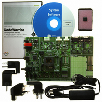
Manufacturer Part Number
EVB9S08DZ60
Description
BOARD EVAL FOR 9S08DZ60
Manufacturer
Freescale Semiconductor
Type
MCUr
Datasheets
1.DEMO9S08DZ60.pdf
(416 pages)
2.EVB9S08DZ60.pdf
(2 pages)
3.EVB9S08DZ60.pdf
(32 pages)
4.EVB9S08DZ60.pdf
(13 pages)
5.EVB9S08DZ60.pdf
(4 pages)
Specifications of EVB9S08DZ60
Contents
Module and Misc Hardware
Processor To Be Evaluated
S08D
Data Bus Width
8 bit
Interface Type
RS-232, USB
Silicon Manufacturer
Freescale
Core Architecture
HCS08
Core Sub-architecture
HCS08
Silicon Core Number
MC9S08
Silicon Family Name
S08D
Kit Contents
Board Cables CD Power Supply
Rohs Compliant
Yes
For Use With/related Products
MC9S08DZ60
Lead Free Status / RoHS Status
Lead free / RoHS Compliant
Available stocks
Company
Part Number
Manufacturer
Quantity
Price
Company:

Part Number:
EVB9S08DZ60
Manufacturer:
TI
Quantity:
101


1
2
3
4
5
6
Appendix A Electrical Characteristics
374
Num
14
15
16
17
18
19
20
21
22
23
24
Typical values are measured at 25°C. Characterized, not tested
When a pin interrupt is configured to detect rising edges, pulldown resistors are used in place of pullup resistors.
Maximum is highest voltage that POR is guaranteed.
Simulated, not tested
Power supply must maintain regulation within operating V
conditions. If positive injection current (V
in external power supply going out of regulation. Ensure external V
current. This will be the greatest risk when the MCU is not consuming power. Examples are: if no system clock is present, or
if clock rate is very low which (would reduce overall power consumption).
All functional non-supply pins are internally clamped to V
D POR re-arm voltage
D POR re-arm time
C
C
D
C
P
P
P
P
T
C
Low-voltage detection threshold —
high range
Low-voltage detection threshold —
low range
Low-voltage warning threshold —
high range 1
Low-voltage warning threshold —
high range 0
Low-voltage warning threshold
low range 1
Low-voltage warning threshold —
low range 0
Low-voltage inhibit reset/recover
hysteresis
dc injection current
Bandgap Voltage Reference
Factory trimmed at
V
DD
= 5.0 V, Temp = 25°C
Characteristic
Total MCU limit, includes
sum of all stressed pins
4
5, 6, 7, 8
3
Single pin limit
Table A-6. DC Characteristics (continued)
V
V
V
V
V
V
V
V
V
V
V
V
In
MC9S08DZ60 Series Data Sheet, Rev. 4
DD
DD
DD
DD
DD
DD
DD
DD
DD
DD
DD
DD
> V
falling
falling
falling
falling
falling
falling
rising
rising
rising
rising
rising
rising
DD
) is greater than I
Symbol
V
V
V
V
V
V
V
t
V
V
POR
LVW3
LVW2
LVW1
LVW0
LVD1
LVD0
POR
I
hys
IC
BG
SS
DD
and V
range during instantaneous and operating maximum current
DD
DD
V
V
Condition
V
DD
V
, the injection current may flow out of V
IN
IN
IN
IN
.
5 V
3 V
load will shunt current greater than maximum injection
> V
< V
> V
< V
DD
DD
SS
SS
2.48
2.54
2.84
2.90
2.66
2.72
1.19
Min
0.9
3.9
4.0
4.5
4.6
4.2
4.3
10
—
—
0
0
0
0
2.56
2.62
2.92
2.98
2.74
2.80
1.20
Typ
100
1.4
4.0
4.1
4.6
4.7
4.3
4.4
60
—
—
—
—
—
Freescale Semiconductor
1
DD
and could result
2.64
2.70
3.00
3.06
2.82
2.88
–0.2
1.21
Max
2.0
4.1
4.2
4.7
4.8
4.4
4.5
25
–5
—
—
—
2
Unit
mV
mA
μs
V
V
V
V
V
V
V
V
Related parts for EVB9S08DZ60
Image
Part Number
Description
Manufacturer
Datasheet
Request
R

Part Number:
Description:
Manufacturer:
Freescale Semiconductor, Inc
Datasheet:
Part Number:
Description:
Manufacturer:
Freescale Semiconductor, Inc
Datasheet:
Part Number:
Description:
Manufacturer:
Freescale Semiconductor, Inc
Datasheet:
Part Number:
Description:
Manufacturer:
Freescale Semiconductor, Inc
Datasheet:
Part Number:
Description:
Manufacturer:
Freescale Semiconductor, Inc
Datasheet:
Part Number:
Description:
Manufacturer:
Freescale Semiconductor, Inc
Datasheet:
Part Number:
Description:
Manufacturer:
Freescale Semiconductor, Inc
Datasheet:
Part Number:
Description:
Manufacturer:
Freescale Semiconductor, Inc
Datasheet:
Part Number:
Description:
Manufacturer:
Freescale Semiconductor, Inc
Datasheet:
Part Number:
Description:
Manufacturer:
Freescale Semiconductor, Inc
Datasheet:
Part Number:
Description:
Manufacturer:
Freescale Semiconductor, Inc
Datasheet:
Part Number:
Description:
Manufacturer:
Freescale Semiconductor, Inc
Datasheet:
Part Number:
Description:
Manufacturer:
Freescale Semiconductor, Inc
Datasheet:
Part Number:
Description:
Manufacturer:
Freescale Semiconductor, Inc
Datasheet:
Part Number:
Description:
Manufacturer:
Freescale Semiconductor, Inc
Datasheet: