EVB9S08DZ60 Freescale Semiconductor, EVB9S08DZ60 Datasheet - Page 286
EVB9S08DZ60
Manufacturer Part Number
EVB9S08DZ60
Description
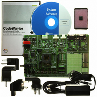
BOARD EVAL FOR 9S08DZ60
Manufacturer
Freescale Semiconductor
Type
MCUr
Datasheets
1.DEMO9S08DZ60.pdf
(416 pages)
2.EVB9S08DZ60.pdf
(2 pages)
3.EVB9S08DZ60.pdf
(32 pages)
4.EVB9S08DZ60.pdf
(13 pages)
5.EVB9S08DZ60.pdf
(4 pages)
Specifications of EVB9S08DZ60
Contents
Module and Misc Hardware
Processor To Be Evaluated
S08D
Data Bus Width
8 bit
Interface Type
RS-232, USB
Silicon Manufacturer
Freescale
Core Architecture
HCS08
Core Sub-architecture
HCS08
Silicon Core Number
MC9S08
Silicon Family Name
S08D
Kit Contents
Board Cables CD Power Supply
Rohs Compliant
Yes
For Use With/related Products
MC9S08DZ60
Lead Free Status / RoHS Status
Lead free / RoHS Compliant
Available stocks
Company
Part Number
Manufacturer
Quantity
Price
Company:

Part Number:
EVB9S08DZ60
Manufacturer:
TI
Quantity:
101


Chapter 13 Serial Peripheral Interface (S08SPIV3)
in LSBFE. Both variations of SPSCK polarity are shown, but only one of these waveforms applies for a
specific transfer, depending on the value in CPOL. The SAMPLE IN waveform applies to the MOSI input
of a slave or the MISO input of a master. The MOSI waveform applies to the MOSI output pin from a
master and the MISO waveform applies to the MISO output from a slave. The SS OUT waveform applies
to the slave select output from a master (provided MODFEN and SSOE = 1). The master SS output goes
to active low at the start of the first bit time of the transfer and goes back high one-half SPSCK cycle after
the end of the eighth bit time of the transfer. The SS IN waveform applies to the slave select input of a
slave.
When CPHA = 0, the slave begins to drive its MISO output with the first data bit value (MSB or LSB
depending on LSBFE) when SS goes to active low. The first SPSCK edge causes both the master and the
slave to sample the data bit values on their MISO and MOSI inputs, respectively. At the second SPSCK
edge, the SPI shifter shifts one bit position which shifts in the bit value that was just sampled and shifts the
second data bit value out the other end of the shifter to the MOSI and MISO outputs of the master and
slave, respectively. When CPHA = 0, the slave’s SS input must go to its inactive high level between
transfers.
286
(MISO OR MOSI)
(MASTER OUT)
(REFERENCE)
(SLAVE OUT)
SAMPLE IN
MSB FIRST
BIT TIME #
(CPOL = 0)
(CPOL = 1)
LSB FIRST
(MASTER)
(SLAVE)
SS OUT
SPSCK
SPSCK
SS IN
MOSI
MISO
BIT 7
BIT 0
1
Figure 13-11. SPI Clock Formats (CPHA = 0)
MC9S08DZ60 Series Data Sheet, Rev. 4
BIT 6
BIT 1
2
...
...
...
BIT 2
BIT 5
6
BIT 1
BIT 6
7
BIT 0
BIT 7
8
Freescale Semiconductor
Related parts for EVB9S08DZ60
Image
Part Number
Description
Manufacturer
Datasheet
Request
R

Part Number:
Description:
Manufacturer:
Freescale Semiconductor, Inc
Datasheet:
Part Number:
Description:
Manufacturer:
Freescale Semiconductor, Inc
Datasheet:
Part Number:
Description:
Manufacturer:
Freescale Semiconductor, Inc
Datasheet:
Part Number:
Description:
Manufacturer:
Freescale Semiconductor, Inc
Datasheet:
Part Number:
Description:
Manufacturer:
Freescale Semiconductor, Inc
Datasheet:
Part Number:
Description:
Manufacturer:
Freescale Semiconductor, Inc
Datasheet:
Part Number:
Description:
Manufacturer:
Freescale Semiconductor, Inc
Datasheet:
Part Number:
Description:
Manufacturer:
Freescale Semiconductor, Inc
Datasheet:
Part Number:
Description:
Manufacturer:
Freescale Semiconductor, Inc
Datasheet:
Part Number:
Description:
Manufacturer:
Freescale Semiconductor, Inc
Datasheet:
Part Number:
Description:
Manufacturer:
Freescale Semiconductor, Inc
Datasheet:
Part Number:
Description:
Manufacturer:
Freescale Semiconductor, Inc
Datasheet:
Part Number:
Description:
Manufacturer:
Freescale Semiconductor, Inc
Datasheet:
Part Number:
Description:
Manufacturer:
Freescale Semiconductor, Inc
Datasheet:
Part Number:
Description:
Manufacturer:
Freescale Semiconductor, Inc
Datasheet: