EVB9S08DZ60 Freescale Semiconductor, EVB9S08DZ60 Datasheet - Page 280
EVB9S08DZ60
Manufacturer Part Number
EVB9S08DZ60
Description
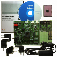
BOARD EVAL FOR 9S08DZ60
Manufacturer
Freescale Semiconductor
Type
MCUr
Datasheets
1.DEMO9S08DZ60.pdf
(416 pages)
2.EVB9S08DZ60.pdf
(2 pages)
3.EVB9S08DZ60.pdf
(32 pages)
4.EVB9S08DZ60.pdf
(13 pages)
5.EVB9S08DZ60.pdf
(4 pages)
Specifications of EVB9S08DZ60
Contents
Module and Misc Hardware
Processor To Be Evaluated
S08D
Data Bus Width
8 bit
Interface Type
RS-232, USB
Silicon Manufacturer
Freescale
Core Architecture
HCS08
Core Sub-architecture
HCS08
Silicon Core Number
MC9S08
Silicon Family Name
S08D
Kit Contents
Board Cables CD Power Supply
Rohs Compliant
Yes
For Use With/related Products
MC9S08DZ60
Lead Free Status / RoHS Status
Lead free / RoHS Compliant
Available stocks
Company
Part Number
Manufacturer
Quantity
Price
Company:

Part Number:
EVB9S08DZ60
Manufacturer:
TI
Quantity:
101


Chapter 13 Serial Peripheral Interface (S08SPIV3)
Ensure that the SPI should not be disabled (SPE=0) at the same time as a bit change to the CPHA bit. These
changes should be performed as separate operations or unexpected behavior may occur.
13.4.2
This read/write register is used to control optional features of the SPI system. Bits 7, 6, 5, and 2 are not
implemented and always read 0.
280
Reset
LSBFE
MSTR
CPHA
SSOE
CPOL
Field
4
3
2
1
0
W
R
SPI Control Register 2 (SPIC2)
Master/Slave Mode Select
0 SPI module configured as a slave SPI device
1 SPI module configured as a master SPI device
Clock Polarity — This bit effectively places an inverter in series with the clock signal from a master SPI or to a
slave SPI device. Refer to
0 Active-high SPI clock (idles low)
1 Active-low SPI clock (idles high)
Clock Phase — This bit selects one of two clock formats for different kinds of synchronous serial peripheral
devices. Refer to
0 First edge on SPSCK occurs at the middle of the first cycle of an 8-cycle data transfer
1 First edge on SPSCK occurs at the start of the first cycle of an 8-cycle data transfer
Slave Select Output Enable — This bit is used in combination with the mode fault enable (MODFEN) bit in
SPCR2 and the master/slave (MSTR) control bit to determine the function of the SS pin as shown in
LSB First (Shifter Direction)
0 SPI serial data transfers start with most significant bit
1 SPI serial data transfers start with least significant bit
MODFEN
0
0
7
0
0
1
1
= Unimplemented or Reserved
0
0
6
Section 13.5.1, “SPI Clock
SSOE
Table 13-1. SPIC1 Field Descriptions (continued)
0
1
0
1
Figure 13-6. SPI Control Register 2 (SPIC2)
Section 13.5.1, “SPI Clock
MC9S08DZ60 Series Data Sheet, Rev. 4
General-purpose I/O (not SPI)
General-purpose I/O (not SPI)
SS input for mode fault
Automatic SS output
0
0
5
Table 13-2. SS Pin Function
MODFEN
Master Mode
NOTE
Formats”
0
4
Description
Formats”
for more details.
BIDIROE
3
0
for more details.
Slave select input
Slave select input
Slave select input
Slave select input
0
0
2
Slave Mode
SPISWAI
Freescale Semiconductor
0
1
Table
SPC0
0
0
13-2.
Related parts for EVB9S08DZ60
Image
Part Number
Description
Manufacturer
Datasheet
Request
R

Part Number:
Description:
Manufacturer:
Freescale Semiconductor, Inc
Datasheet:
Part Number:
Description:
Manufacturer:
Freescale Semiconductor, Inc
Datasheet:
Part Number:
Description:
Manufacturer:
Freescale Semiconductor, Inc
Datasheet:
Part Number:
Description:
Manufacturer:
Freescale Semiconductor, Inc
Datasheet:
Part Number:
Description:
Manufacturer:
Freescale Semiconductor, Inc
Datasheet:
Part Number:
Description:
Manufacturer:
Freescale Semiconductor, Inc
Datasheet:
Part Number:
Description:
Manufacturer:
Freescale Semiconductor, Inc
Datasheet:
Part Number:
Description:
Manufacturer:
Freescale Semiconductor, Inc
Datasheet:
Part Number:
Description:
Manufacturer:
Freescale Semiconductor, Inc
Datasheet:
Part Number:
Description:
Manufacturer:
Freescale Semiconductor, Inc
Datasheet:
Part Number:
Description:
Manufacturer:
Freescale Semiconductor, Inc
Datasheet:
Part Number:
Description:
Manufacturer:
Freescale Semiconductor, Inc
Datasheet:
Part Number:
Description:
Manufacturer:
Freescale Semiconductor, Inc
Datasheet:
Part Number:
Description:
Manufacturer:
Freescale Semiconductor, Inc
Datasheet:
Part Number:
Description:
Manufacturer:
Freescale Semiconductor, Inc
Datasheet: