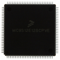
MC9S12E128CPVE Freescale Semiconductor, MC9S12E128CPVE Datasheet - Page 252

MC9S12E128CPVE
Manufacturer Part Number
MC9S12E128CPVE
Description
IC MCU 128K FLASH 25MHZ 112-LQFP
Manufacturer
Freescale Semiconductor
Series
HCS12r
Specifications of MC9S12E128CPVE
Core Processor
HCS12
Core Size
16-Bit
Speed
25MHz
Connectivity
EBI/EMI, I²C, SCI, SPI
Peripherals
POR, PWM, WDT
Number Of I /o
91
Program Memory Size
128KB (128K x 8)
Program Memory Type
FLASH
Ram Size
8K x 8
Voltage - Supply (vcc/vdd)
2.35 V ~ 2.75 V
Data Converters
A/D 16x10b; D/A 2x8b
Oscillator Type
Internal
Operating Temperature
-40°C ~ 85°C
Package / Case
112-LQFP
Processor Series
S12E
Core
HCS12
Data Bus Width
16 bit
Data Ram Size
8 KB
Interface Type
SCI/SPI
Maximum Clock Frequency
25 MHz
Number Of Programmable I/os
92
Number Of Timers
12
Operating Supply Voltage
3.135 V to 5.5 V
Maximum Operating Temperature
+ 85 C
Mounting Style
SMD/SMT
3rd Party Development Tools
EWHCS12
Minimum Operating Temperature
- 40 C
On-chip Adc
16-ch x 10-bit
On-chip Dac
2-ch x 8-bit
Controller Family/series
HCS12/S12X
No. Of I/o's
90
Ram Memory Size
8KB
Cpu Speed
25MHz
No. Of Timers
4
Embedded Interface Type
I2C, SCI, SPI
Rohs Compliant
Yes
For Use With
M68EVB912E128 - BOARD EVAL FOR MC9S12E128/64
Lead Free Status / RoHS Status
Lead free / RoHS Compliant
Eeprom Size
-
Lead Free Status / Rohs Status
Lead free / RoHS Compliant
Available stocks
Company
Part Number
Manufacturer
Quantity
Price
Company:
Part Number:
MC9S12E128CPVE
Manufacturer:
Freescale Semiconductor
Quantity:
10 000
- Current page: 252 of 606
- Download datasheet (4Mb)
Chapter 8 Serial Communication Interface (SCIV3)
252
SCISWAI
LOOPS
WAKE
RSRC
Field
ILT
PE
PT
M
7
6
5
4
3
2
1
0
LOOPS
Loop Select Bit — LOOPS enables loop operation. In loop operation, the RXD pin is disconnected from the SCI
and the transmitter output is internally connected to the receiver input. Both the transmitter and the receiver must
be enabled to use the loop function.
0 Normal operation enabled
1 Loop operation enabled
The receiver input is determined by the RSRC bit.
SCI Stop in Wait Mode Bit — SCISWAI disables the SCI in wait mode.
0 SCI enabled in wait mode
1 SCI disabled in wait mode
Receiver Source Bit — When LOOPS = 1, the RSRC bit determines the source for the receiver shift register
input.
0 Receiver input internally connected to transmitter output
1 Receiver input connected externally to transmitter
Refer to
Data Format Mode Bit — MODE determines whether data characters are eight or nine bits long.
0 One start bit, eight data bits, one stop bit
1 One start bit, nine data bits, one stop bit
Wakeup Condition Bit — WAKE determines which condition wakes up the SCI: a logic 1 (address mark) in the
most significant bit position of a received data character or an idle condition on the RXD pin.
0 Idle line wakeup
1 Address mark wakeup
Idle Line Type Bit — ILT determines when the receiver starts counting logic 1s as idle character bits. The
counting begins either after the start bit or after the stop bit. If the count begins after the start bit, then a string of
logic 1s preceding the stop bit may cause false recognition of an idle character. Beginning the count after the
stop bit avoids false idle character recognition, but requires properly synchronized transmissions.
0 Idle character bit count begins after start bit
1 Idle character bit count begins after stop bit
Parity Enable Bit — PE enables the parity function. When enabled, the parity function inserts a parity bit in the
most significant bit position.
0 Parity function disabled
1 Parity function enabled
Parity Type Bit — PT determines whether the SCI generates and checks for even parity or odd parity. With even
parity, an even number of 1s clears the parity bit and an odd number of 1s sets the parity bit. With odd parity, an
odd number of 1s clears the parity bit and an even number of 1s sets the parity bit.
0 Even parity
1 Odd parity
0
1
1
Table
RSRC
x
0
1
8-5.
Normal operation
Loop mode with transmitter output internally connected to receiver input
Single-wire mode with TXD pin connected to receiver input
Table 8-4. SCICR1 Field Descriptions
MC9S12E128 Data Sheet, Rev. 1.07
Table 8-5. Loop Functions
Description
Function
Freescale Semiconductor
Related parts for MC9S12E128CPVE
Image
Part Number
Description
Manufacturer
Datasheet
Request
R
Part Number:
Description:
Manufacturer:
Freescale Semiconductor, Inc
Datasheet:
Part Number:
Description:
Manufacturer:
Freescale Semiconductor, Inc
Datasheet:
Part Number:
Description:
Manufacturer:
Freescale Semiconductor, Inc
Datasheet:
Part Number:
Description:
Manufacturer:
Freescale Semiconductor, Inc
Datasheet:
Part Number:
Description:
Manufacturer:
Freescale Semiconductor, Inc
Datasheet:
Part Number:
Description:
Manufacturer:
Freescale Semiconductor, Inc
Datasheet:
Part Number:
Description:
Manufacturer:
Freescale Semiconductor, Inc
Datasheet:
Part Number:
Description:
Manufacturer:
Freescale Semiconductor, Inc
Datasheet:
Part Number:
Description:
Manufacturer:
Freescale Semiconductor, Inc
Datasheet:
Part Number:
Description:
Manufacturer:
Freescale Semiconductor, Inc
Datasheet:
Part Number:
Description:
Manufacturer:
Freescale Semiconductor, Inc
Datasheet:
Part Number:
Description:
Manufacturer:
Freescale Semiconductor, Inc
Datasheet:
Part Number:
Description:
Manufacturer:
Freescale Semiconductor, Inc
Datasheet:
Part Number:
Description:
Manufacturer:
Freescale Semiconductor, Inc
Datasheet:
Part Number:
Description:
Manufacturer:
Freescale Semiconductor, Inc
Datasheet:


