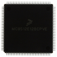
MC9S12E128CPVE Freescale Semiconductor, MC9S12E128CPVE Datasheet - Page 318

MC9S12E128CPVE
Manufacturer Part Number
MC9S12E128CPVE
Description
IC MCU 128K FLASH 25MHZ 112-LQFP
Manufacturer
Freescale Semiconductor
Series
HCS12r
Specifications of MC9S12E128CPVE
Core Processor
HCS12
Core Size
16-Bit
Speed
25MHz
Connectivity
EBI/EMI, I²C, SCI, SPI
Peripherals
POR, PWM, WDT
Number Of I /o
91
Program Memory Size
128KB (128K x 8)
Program Memory Type
FLASH
Ram Size
8K x 8
Voltage - Supply (vcc/vdd)
2.35 V ~ 2.75 V
Data Converters
A/D 16x10b; D/A 2x8b
Oscillator Type
Internal
Operating Temperature
-40°C ~ 85°C
Package / Case
112-LQFP
Processor Series
S12E
Core
HCS12
Data Bus Width
16 bit
Data Ram Size
8 KB
Interface Type
SCI/SPI
Maximum Clock Frequency
25 MHz
Number Of Programmable I/os
92
Number Of Timers
12
Operating Supply Voltage
3.135 V to 5.5 V
Maximum Operating Temperature
+ 85 C
Mounting Style
SMD/SMT
3rd Party Development Tools
EWHCS12
Minimum Operating Temperature
- 40 C
On-chip Adc
16-ch x 10-bit
On-chip Dac
2-ch x 8-bit
Controller Family/series
HCS12/S12X
No. Of I/o's
90
Ram Memory Size
8KB
Cpu Speed
25MHz
No. Of Timers
4
Embedded Interface Type
I2C, SCI, SPI
Rohs Compliant
Yes
For Use With
M68EVB912E128 - BOARD EVAL FOR MC9S12E128/64
Lead Free Status / RoHS Status
Lead free / RoHS Compliant
Eeprom Size
-
Lead Free Status / Rohs Status
Lead free / RoHS Compliant
Available stocks
Company
Part Number
Manufacturer
Quantity
Price
Company:
Part Number:
MC9S12E128CPVE
Manufacturer:
Freescale Semiconductor
Quantity:
10 000
- Current page: 318 of 606
- Download datasheet (4Mb)
Chapter 10 Inter-Integrated Circuit (IICV2)
10.7.1.2
After completion of the initialization procedure, serial data can be transmitted by selecting the 'master
transmitter' mode. If the device is connected to a multi-master bus system, the state of the IIC bus busy bit
(IBB) must be tested to check whether the serial bus is free.
If the bus is free (IBB=0), the start condition and the first byte (the slave address) can be sent. The data
written to the data register comprises the slave calling address and the LSB set to indicate the direction of
transfer required from the slave.
The bus free time (i.e., the time between a STOP condition and the following START condition) is built
into the hardware that generates the START cycle. Depending on the relative frequencies of the system
clock and the SCL period it may be necessary to wait until the IIC is busy after writing the calling address
to the IBDR before proceeding with the following instructions. This is illustrated in the following example.
An example of a program which generates the START signal and transmits the first byte of data (slave
address) is shown below:
10.7.1.3
Transmission or reception of a byte will set the data transferring bit (TCF) to 1, which indicates one byte
communication is finished. The IIC bus interrupt bit (IBIF) is set also; an interrupt will be generated if the
interrupt function is enabled during initialization by setting the IBIE bit. Software must clear the IBIF bit
in the interrupt routine first. The TCF bit will be cleared by reading from the IIC bus data I/O register
(IBDR) in receive mode or writing to IBDR in transmit mode.
Software may service the IIC I/O in the main program by monitoring the IBIF bit if the interrupt function
is disabled. Note that polling should monitor the IBIF bit rather than the TCF bit because their operation
is different when arbitration is lost.
Note that when an interrupt occurs at the end of the address cycle the master will always be in transmit
mode, i.e. the address is transmitted. If master receive mode is required, indicated by R/W bit in IBDR,
then the Tx/Rx bit should be toggled at this stage.
During slave mode address cycles (IAAS=1), the SRW bit in the status register is read to determine the
direction of the subsequent transfer and the Tx/Rx bit is programmed accordingly. For slave mode data
cycles (IAAS=0) the SRW bit is not valid, the Tx/Rx bit in the control register should be read to determine
the direction of the current transfer.
The following is an example of a software response by a 'master transmitter' in the interrupt routine.
318
ISR
TRANSMIT
CHFLAG
TXSTART
IBFREE
BCLR
BRCLR
BRCLR
BRSET
MOVB
Generation of START
Post-Transfer Software Response
BRSET
BSET
MOVB
BRCLR
IBSR,#$02
IBCR,#$20,SLAVE
IBCR,#$10,RECEIVE
IBSR,#$01,END
DATABUF,IBDR
IBSR,#$20,*
IBCR,#$30
CALLING,IBDR
IBSR,#$20,*
MC9S12E128 Data Sheet, Rev. 1.07
;WAIT FOR IBB FLAG TO CLEAR
;SET TRANSMIT AND MASTER MODE;i.e. GENERATE START CONDITION
;TRANSMIT THE CALLING ADDRESS, D0=R/W
;WAIT FOR IBB FLAG TO SET
;CLEAR THE IBIF FLAG
;BRANCH IF IN SLAVE MODE
;BRANCH IF IN RECEIVE MODE
;IF NO ACK, END OF TRANSMISSION
;TRANSMIT NEXT BYTE OF DATA
Freescale Semiconductor
Related parts for MC9S12E128CPVE
Image
Part Number
Description
Manufacturer
Datasheet
Request
R
Part Number:
Description:
Manufacturer:
Freescale Semiconductor, Inc
Datasheet:
Part Number:
Description:
Manufacturer:
Freescale Semiconductor, Inc
Datasheet:
Part Number:
Description:
Manufacturer:
Freescale Semiconductor, Inc
Datasheet:
Part Number:
Description:
Manufacturer:
Freescale Semiconductor, Inc
Datasheet:
Part Number:
Description:
Manufacturer:
Freescale Semiconductor, Inc
Datasheet:
Part Number:
Description:
Manufacturer:
Freescale Semiconductor, Inc
Datasheet:
Part Number:
Description:
Manufacturer:
Freescale Semiconductor, Inc
Datasheet:
Part Number:
Description:
Manufacturer:
Freescale Semiconductor, Inc
Datasheet:
Part Number:
Description:
Manufacturer:
Freescale Semiconductor, Inc
Datasheet:
Part Number:
Description:
Manufacturer:
Freescale Semiconductor, Inc
Datasheet:
Part Number:
Description:
Manufacturer:
Freescale Semiconductor, Inc
Datasheet:
Part Number:
Description:
Manufacturer:
Freescale Semiconductor, Inc
Datasheet:
Part Number:
Description:
Manufacturer:
Freescale Semiconductor, Inc
Datasheet:
Part Number:
Description:
Manufacturer:
Freescale Semiconductor, Inc
Datasheet:
Part Number:
Description:
Manufacturer:
Freescale Semiconductor, Inc
Datasheet:


