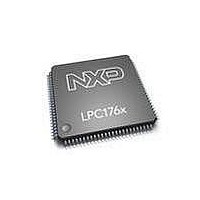
LPC1759FBD80,551 NXP Semiconductors, LPC1759FBD80,551 Datasheet - Page 68

LPC1759FBD80,551
Manufacturer Part Number
LPC1759FBD80,551
Description
IC ARM CORTEX MCU 512K 80-LQFP
Manufacturer
NXP Semiconductors
Series
LPC17xxr
Datasheets
1.LPC1751FBD80551.pdf
(74 pages)
2.LPC1767FBD100551.pdf
(2 pages)
3.LPC1767FBD100551.pdf
(840 pages)
Specifications of LPC1759FBD80,551
Program Memory Type
FLASH
Program Memory Size
512KB (512K x 8)
Package / Case
80-LQFP
Core Processor
ARM® Cortex-M3™
Core Size
32-Bit
Speed
120MHz
Connectivity
CAN, I²C, IrDA, Microwire, SPI, SSI, SSP, UART/USART, USB OTG
Peripherals
Brown-out Detect/Reset, DMA, I²S, Motor Control PWM, POR, PWM, WDT
Number Of I /o
52
Ram Size
64K x 8
Voltage - Supply (vcc/vdd)
2.4 V ~ 3.6 V
Data Converters
A/D 6x12b, D/A 1x10b
Oscillator Type
Internal
Operating Temperature
-40°C ~ 85°C
Processor Series
LPC17
Core
ARM Cortex M3
Data Bus Width
32 bit
Data Ram Size
64 KB
Interface Type
Ethernet, USB, OTG, CAN
Maximum Clock Frequency
120 MHz
Number Of Programmable I/os
52
Number Of Timers
4
Operating Supply Voltage
3.3 V
Maximum Operating Temperature
+ 85 C
Mounting Style
SMD/SMT
3rd Party Development Tools
MDK-ARM, RL-ARM, ULINK2
Minimum Operating Temperature
- 40 C
On-chip Adc
12 bit, 6 Channel
On-chip Dac
10 bit
Package
80LQFP
Device Core
ARM Cortex M3
Family Name
LPC17xx
Maximum Speed
120 MHz
Lead Free Status / RoHS Status
Lead free / RoHS Compliant
For Use With
622-1005 - USB IN-CIRCUIT PROG ARM7 LPC2K
Eeprom Size
-
Lead Free Status / Rohs Status
Lead free / RoHS Compliant
Other names
568-4968
935290523551
935290523551
Available stocks
Company
Part Number
Manufacturer
Quantity
Price
Company:
Part Number:
LPC1759FBD80,551
Manufacturer:
LT
Quantity:
375
Company:
Part Number:
LPC1759FBD80,551
Manufacturer:
NXP Semiconductors
Quantity:
10 000
Part Number:
LPC1759FBD80,551
Manufacturer:
NXP/恩智浦
Quantity:
20 000
- Current page: 68 of 840
- Download datasheet (6Mb)
5.1 Introduction
5.2 Flash accelerator blocks
UM10360
User manual
Fig 13. Simplified block diagram of the flash accelerator showing potential bus connections
Cortex-M3
Controller
Purpose
General
5.2.1 Flash memory bank
DMA
CPU
Master Port
The flash accelerator block in the LPC17xx allows maximization of the performance of the
Cortex-M3 processor when it is running code from flash memory, while also saving power.
The flash accelerator also provides speed and power improvements for data accesses to
the flash memory.
The flash accelerator is divided into several functional blocks:
Figure 13
In the following descriptions, the term “fetch” applies to an explicit flash read request from
the CPU. “Prefetch” is used to denote a flash read of instructions beyond the current
processor fetch address.
There is one bank of flash memory controlled by the LPC17xx flash accelerator.
Flash programming operations are not controlled by the flash accelerator, but are handled
as a separate function. A Boot ROM contains flash programming algorithms that may be
called as part of the application program, and a loader that may be run to allow
programming of the flash memory.
DCode
•
•
•
•
ICode
DMA
bus
bus
UM10360
Chapter 5: LPC17xx Flash accelerator
Rev. 2 — 19 August 2010
AHB-Lite bus interface, accessible by the Cortex-M3 I-code and D-code buses, as
well as by the General Purpose DMA Controller
An array of eight 128-bit buffers
Flash accelerator control logic, including address compare and flash control
A flash memory interface
Matrix
shows a simplified diagram of the flash accelerator blocks and data paths.
Bus
Combined
All information provided in this document is subject to legal disclaimers.
AHB
Rev. 2 — 19 August 2010
Flash Accelerator
bus interface
AHB-Lite
Accelerator
Control
Buffer
Array
Flash
Interface
Flash
Memory
Flash
© NXP B.V. 2010. All rights reserved.
User manual
68 of 840
Related parts for LPC1759FBD80,551
Image
Part Number
Description
Manufacturer
Datasheet
Request
R
Part Number:
Description:
Lpc17xx Device Highlight
Manufacturer:
NXP Semiconductors
Datasheet:
Part Number:
Description:
NXP Semiconductors designed the LPC2420/2460 microcontroller around a 16-bit/32-bitARM7TDMI-S CPU core with real-time debug interfaces that include both JTAG andembedded trace
Manufacturer:
NXP Semiconductors
Datasheet:

Part Number:
Description:
NXP Semiconductors designed the LPC2458 microcontroller around a 16-bit/32-bitARM7TDMI-S CPU core with real-time debug interfaces that include both JTAG andembedded trace
Manufacturer:
NXP Semiconductors
Datasheet:
Part Number:
Description:
NXP Semiconductors designed the LPC2468 microcontroller around a 16-bit/32-bitARM7TDMI-S CPU core with real-time debug interfaces that include both JTAG andembedded trace
Manufacturer:
NXP Semiconductors
Datasheet:
Part Number:
Description:
NXP Semiconductors designed the LPC2470 microcontroller, powered by theARM7TDMI-S core, to be a highly integrated microcontroller for a wide range ofapplications that require advanced communications and high quality graphic displays
Manufacturer:
NXP Semiconductors
Datasheet:
Part Number:
Description:
NXP Semiconductors designed the LPC2478 microcontroller, powered by theARM7TDMI-S core, to be a highly integrated microcontroller for a wide range ofapplications that require advanced communications and high quality graphic displays
Manufacturer:
NXP Semiconductors
Datasheet:
Part Number:
Description:
The Philips Semiconductors XA (eXtended Architecture) family of 16-bit single-chip microcontrollers is powerful enough to easily handle the requirements of high performance embedded applications, yet inexpensive enough to compete in the market for hi
Manufacturer:
NXP Semiconductors
Datasheet:
Part Number:
Description:
The XA-S3 device is a member of Philips Semiconductors? XA(eXtended Architecture) family of high performance 16-bitsingle-chip microcontrollers
Manufacturer:
NXP Semiconductors
Datasheet:

Part Number:
Description:
The NXP BlueStreak LH75401/LH75411 family consists of two low-cost 16/32-bit System-on-Chip (SoC) devices
Manufacturer:
NXP Semiconductors
Datasheet:

Part Number:
Description:
The NXP LPC3130/3131 combine an 180 MHz ARM926EJ-S CPU core, high-speed USB2
Manufacturer:
NXP Semiconductors
Datasheet:

Part Number:
Description:
The NXP LPC3141 combine a 270 MHz ARM926EJ-S CPU core, High-speed USB 2
Manufacturer:
NXP Semiconductors

Part Number:
Description:
The NXP LPC3143 combine a 270 MHz ARM926EJ-S CPU core, High-speed USB 2
Manufacturer:
NXP Semiconductors

Part Number:
Description:
The NXP LPC3152 combines an 180 MHz ARM926EJ-S CPU core, High-speed USB 2
Manufacturer:
NXP Semiconductors

Part Number:
Description:
The NXP LPC3154 combines an 180 MHz ARM926EJ-S CPU core, High-speed USB 2
Manufacturer:
NXP Semiconductors


