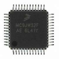
MCHC908JW32FAE Freescale Semiconductor, MCHC908JW32FAE Datasheet - Page 104

MCHC908JW32FAE
Manufacturer Part Number
MCHC908JW32FAE
Description
IC MCU 32K FLASH 8MHZ 48-LQFP
Manufacturer
Freescale Semiconductor
Series
HC08r
Datasheet
1.RD3152MMA7260Q.pdf
(232 pages)
Specifications of MCHC908JW32FAE
Core Processor
HC08
Core Size
8-Bit
Speed
8MHz
Connectivity
SPI, USB
Peripherals
LED, LVD, POR, PWM
Number Of I /o
29
Program Memory Size
32KB (32K x 8)
Program Memory Type
FLASH
Ram Size
1K x 8
Voltage - Supply (vcc/vdd)
3.5 V ~ 5.5 V
Oscillator Type
Internal
Operating Temperature
0°C ~ 70°C
Package / Case
48-LQFP
Controller Family/series
HC08
No. Of I/o's
48
Ram Memory Size
1KB
Cpu Speed
8MHz
No. Of Timers
1
Embedded Interface Type
SPI
Rohs Compliant
Yes
Processor Series
HC08JW
Core
HC08
Data Bus Width
8 bit
Data Ram Size
1 KB
Interface Type
SPI, USB
Number Of Programmable I/os
29
Number Of Timers
2
Maximum Operating Temperature
+ 70 C
Mounting Style
SMD/SMT
Development Tools By Supplier
FSICEBASE, DEMO908GZ60E, M68EML08GZE, KITUSBSPIDGLEVME, KITUSBSPIEVME, KIT33810EKEVME
Minimum Operating Temperature
0 C
Lead Free Status / RoHS Status
Lead free / RoHS Compliant
Eeprom Size
-
Data Converters
-
Lead Free Status / Rohs Status
Details
Available stocks
Company
Part Number
Manufacturer
Quantity
Price
Company:
Part Number:
MCHC908JW32FAE
Manufacturer:
Freescale Semiconductor
Quantity:
10 000
Part Number:
MCHC908JW32FAE
Manufacturer:
FREESCALE
Quantity:
20 000
Monitor Mode (MON)
The control and data bytes are described below.
7.5.1 PRGRNGE
PRGRNGE is used to program a range of FLASH locations with data loaded into the data array.
The start location of the FLASH to be programmed is specified by the address ADDRH:ADDRL and the
number of bytes from this location is specified by DATASIZE. The maximum number of bytes that can be
programmed in one routine call is 255 bytes (max. DATASIZE is 255).
ADDRH:ADDRL do not need to be at a page boundary, the routine handles any boundary misalignment
during programming. A check to see that all bytes in the specified range are erased is not performed by
this routine prior programming. Nor does this routine do a verification after programming, so there is no
return confirmation that programming was successful. User must assure that the range specified is first
erased.
The coding example below is to program 64 bytes of data starting at FLASH location $EE00, with a bus
speed of 4.9152 MHz. The coding assumes the data block is already loaded in RAM, with the address
pointer, FILE_PTR, pointing to the first byte of the data block.
104
•
•
•
•
Bus speed — This one byte indicates the operating bus speed of the MCU. The value of this byte
should be equal to 4 times the bus speed. E.g. for a 4MHz bus, the value is 16 ($10). This control
byte is useful where the MCU clock source is switched between the PLL clock and the crystal clock.
Data size — This one byte indicates the number of bytes in the data array that are to be
manipulated. The maximum data array size is 255. Routines ERARNGE and MON_ERARNGE do
not manipulate a data array, thus, this data size byte has no meaning.
Start address — These two bytes, high byte followed by low byte, indicate the start address of the
FLASH memory to be manipulated.
Data array — This data array contains data that are to be manipulated. Data in this array are
programmed to FLASH memory by the programming routines: PRGRNGE, MON_PRGRNGE. For
the read routines: LDRNGE and data is read from FLASH and stored in this array.
Routine Description
Data Block Format
Calling Address
Routine Name
Stack Used
Table 7-11. PRGRNGE Routine
MC68HC908JW32 Data Sheet, Rev. 6
PRGRNGE
Program a range of locations
$FE10
16 bytes
Bus speed (BUS_SPD)
Data size (DATASIZE)
Start address high (ADDRH)
Start address (ADDRL)
Data 1 (DATA1)
Data N (DATAN)
:
Freescale Semiconductor


