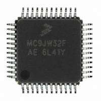
MCHC908JW32FAE Freescale Semiconductor, MCHC908JW32FAE Datasheet - Page 59

MCHC908JW32FAE
Manufacturer Part Number
MCHC908JW32FAE
Description
IC MCU 32K FLASH 8MHZ 48-LQFP
Manufacturer
Freescale Semiconductor
Series
HC08r
Datasheet
1.RD3152MMA7260Q.pdf
(232 pages)
Specifications of MCHC908JW32FAE
Core Processor
HC08
Core Size
8-Bit
Speed
8MHz
Connectivity
SPI, USB
Peripherals
LED, LVD, POR, PWM
Number Of I /o
29
Program Memory Size
32KB (32K x 8)
Program Memory Type
FLASH
Ram Size
1K x 8
Voltage - Supply (vcc/vdd)
3.5 V ~ 5.5 V
Oscillator Type
Internal
Operating Temperature
0°C ~ 70°C
Package / Case
48-LQFP
Controller Family/series
HC08
No. Of I/o's
48
Ram Memory Size
1KB
Cpu Speed
8MHz
No. Of Timers
1
Embedded Interface Type
SPI
Rohs Compliant
Yes
Processor Series
HC08JW
Core
HC08
Data Bus Width
8 bit
Data Ram Size
1 KB
Interface Type
SPI, USB
Number Of Programmable I/os
29
Number Of Timers
2
Maximum Operating Temperature
+ 70 C
Mounting Style
SMD/SMT
Development Tools By Supplier
FSICEBASE, DEMO908GZ60E, M68EML08GZE, KITUSBSPIDGLEVME, KITUSBSPIEVME, KIT33810EKEVME
Minimum Operating Temperature
0 C
Lead Free Status / RoHS Status
Lead free / RoHS Compliant
Eeprom Size
-
Data Converters
-
Lead Free Status / Rohs Status
Details
Available stocks
Company
Part Number
Manufacturer
Quantity
Price
Company:
Part Number:
MCHC908JW32FAE
Manufacturer:
Freescale Semiconductor
Quantity:
10 000
Part Number:
MCHC908JW32FAE
Manufacturer:
FREESCALE
Quantity:
20 000
5.3.1 Oscillator Module
The oscillator module provides two clock outputs CGMXCLK and CGMRCLK to the CGM module.
CGMXCLK when selected, is driven to SIM module to generate the system bus clock. CGMRCLK is used
by the phase-lock-loop to provide a higher frequency system bus clock. The oscillator module also
provides the reference clock for the timebase module (TBM). See
detailed description on TBM.
5.3.2 Phase-Locked Loop Circuit (PLL)
The PLL is a frequency generator that can operate in either acquisition mode or tracking mode, depending
on the accuracy of the output frequency. The PLL can change between acquisition and tracking modes
either automatically or manually.
Freescale Semiconductor
$1090
$1091
$1092
$1093
$1094
$1095
Addr.
NOTES:
1. When AUTO = 0, PLLIE is forced clear and is read-only.
2. When AUTO = 0, PLLF and LOCK read as clear.
3. When AUTO = 1, ACQ is read-only.
4. When PLLON = 0 or VRS7:VRS0 = $0, BCS is forced clear and is read-only.
5. When PLLON = 1, the PLL programming register is read-only.
6. When BCS = 1, PLLON is forced set and is read-only.
PLL Multiplier Select Register
PLL Reference Divider Select
1095PLL VCO Range Select
PLL Bandwidth Control
Register Name
PLL Control Register
PLL Multiplier Select
Register (PMRS)
Register (PMDS)
Register High
Low (PMSL)
Register
(PBWC)
(PMSH)
(PTCL)
Reset:
Reset:
Reset:
Reset:
Reset:
Reset:
Read:
Read:
Read:
Read:
Read:
Read:
Write:
Write:
Write:
Write:
Write:
Write:
Figure 5-2. CGM I/O Register Summary
PLLIE
AUTO
MUL7
VRS7
Bit 7
MC68HC908JW32 Data Sheet, Rev. 6
0
0
0
0
0
0
0
0
= Unimplemented
LOCK
MUL6
VRS6
PLLF
6
0
0
0
0
1
1
0
0
PLLON
MUL5
VRS5
ACQ
5
1
0
0
0
0
0
0
0
MUL4
VRS4
BCS
4
0
0
0
0
0
0
0
0
0
Chapter 9 Timebase Module (TBM)
MUL11
MUL3
RDS3
PRE1
VRS3
R
3
0
0
0
0
0
0
0
= Reserved
MUL10
MUL2
VRS2
RDS2
PRE0
2
0
0
0
0
0
0
0
Functional Description
VPR1
MUL9
MUL1
VRS1
RDS1
1
0
0
0
0
0
0
0
VPR0
MUL8
MUL0
VRS0
RDS0
Bit 0
R
0
0
0
0
1
for
59


