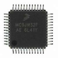
MCHC908JW32FAE Freescale Semiconductor, MCHC908JW32FAE Datasheet - Page 180

MCHC908JW32FAE
Manufacturer Part Number
MCHC908JW32FAE
Description
IC MCU 32K FLASH 8MHZ 48-LQFP
Manufacturer
Freescale Semiconductor
Series
HC08r
Datasheet
1.RD3152MMA7260Q.pdf
(232 pages)
Specifications of MCHC908JW32FAE
Core Processor
HC08
Core Size
8-Bit
Speed
8MHz
Connectivity
SPI, USB
Peripherals
LED, LVD, POR, PWM
Number Of I /o
29
Program Memory Size
32KB (32K x 8)
Program Memory Type
FLASH
Ram Size
1K x 8
Voltage - Supply (vcc/vdd)
3.5 V ~ 5.5 V
Oscillator Type
Internal
Operating Temperature
0°C ~ 70°C
Package / Case
48-LQFP
Controller Family/series
HC08
No. Of I/o's
48
Ram Memory Size
1KB
Cpu Speed
8MHz
No. Of Timers
1
Embedded Interface Type
SPI
Rohs Compliant
Yes
Processor Series
HC08JW
Core
HC08
Data Bus Width
8 bit
Data Ram Size
1 KB
Interface Type
SPI, USB
Number Of Programmable I/os
29
Number Of Timers
2
Maximum Operating Temperature
+ 70 C
Mounting Style
SMD/SMT
Development Tools By Supplier
FSICEBASE, DEMO908GZ60E, M68EML08GZE, KITUSBSPIDGLEVME, KITUSBSPIEVME, KIT33810EKEVME
Minimum Operating Temperature
0 C
Lead Free Status / RoHS Status
Lead free / RoHS Compliant
Eeprom Size
-
Data Converters
-
Lead Free Status / Rohs Status
Details
Available stocks
Company
Part Number
Manufacturer
Quantity
Price
Company:
Part Number:
MCHC908JW32FAE
Manufacturer:
Freescale Semiconductor
Quantity:
10 000
Part Number:
MCHC908JW32FAE
Manufacturer:
FREESCALE
Quantity:
20 000
Input/Output (I/O) Ports
D– and D+ — USB Data Pins
SS, MISO, MOSI, and SPSCK — SPI Functional Pins
13.6.2 Data Direction Register E
Data direction register E determines whether each port E pin is an input or an output. Writing a logic 1 to
a DDRE bit enables the output buffer for the corresponding port E pin; a logic 0 disables the output buffer.
DDRE[7:2] — Data Direction Register E Bits
180
PTE3 pin functions as an external interrupt when PTE3IE=1 in the IRQ option control register (IOCR)
and USBEN=0 in the USB address register (USB disabled). (See
Register.)
PTE2 pin also muxed with PS2 clock generator module. (See
(PS2CLK).)
D– and D+ are the differential data lines used by the USB module. (See
Module.)
When the USB module is enabled, PTE2/D+ and PTE3/D– function as USB data pins D– and D+.
When the USB module is disabled, PTE2/D+ and PTE3/D– function as open drain high current pins
for PS/2 clock and data use.
These are the chip select, master-input-slave-output, master-output-slave-input and clock pins for the
SPI module. The SPI enable bit, SPE, in the SPI control register, SPCR, enables these pins as the SPI
functional pins and overrides any control from port I/O logic. See
Module
These read/write bits control port E data direction. Reset clears DDRE[7:2], configuring all port E pins
as inputs.
1 = Corresponding port E pin configured as output
0 = Corresponding port E pin configured as input
(SPI).
Address:
PTE2/D+ pin has two programmable pullup resistors. One is used for PTE2
when the USB module is disable and another is used for D+ when the USB
module is enabled.
Data direction register E (DDRE) does not affect the data direction of port E
pins that are being used by the SPI module. However, the DDRE bits
always determine whether reading port E returns the states of the latches
or the states of the pins. (See
Avoid glitches on port E pins by writing to the port E data register before
changing data direction register E bits from 0 to 1.
Reset:
Read:
Write:
DDRE7
$0009
Bit 7
0
Figure 13-15. Data Direction Register E (DDRE)
= Unimplemented
DDRE6
6
0
MC68HC908JW32 Data Sheet, Rev. 6
DDRE5
5
0
Table 13-5 . Port C Pin
NOTE
NOTE
DDRE4
4
0
DDRE3
3
0
Chapter 12 PS2 Clock Generator
Chapter 10 Serial Peripheral Interface
DDRE2
Functions.)
14.7 IRQ Status and Control
2
0
Chapter 11 USB 2.0 FS
1
0
Freescale Semiconductor
Bit 0
0


