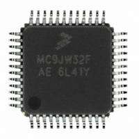
MCHC908JW32FAE Freescale Semiconductor, MCHC908JW32FAE Datasheet - Page 67

MCHC908JW32FAE
Manufacturer Part Number
MCHC908JW32FAE
Description
IC MCU 32K FLASH 8MHZ 48-LQFP
Manufacturer
Freescale Semiconductor
Series
HC08r
Datasheet
1.RD3152MMA7260Q.pdf
(232 pages)
Specifications of MCHC908JW32FAE
Core Processor
HC08
Core Size
8-Bit
Speed
8MHz
Connectivity
SPI, USB
Peripherals
LED, LVD, POR, PWM
Number Of I /o
29
Program Memory Size
32KB (32K x 8)
Program Memory Type
FLASH
Ram Size
1K x 8
Voltage - Supply (vcc/vdd)
3.5 V ~ 5.5 V
Oscillator Type
Internal
Operating Temperature
0°C ~ 70°C
Package / Case
48-LQFP
Controller Family/series
HC08
No. Of I/o's
48
Ram Memory Size
1KB
Cpu Speed
8MHz
No. Of Timers
1
Embedded Interface Type
SPI
Rohs Compliant
Yes
Processor Series
HC08JW
Core
HC08
Data Bus Width
8 bit
Data Ram Size
1 KB
Interface Type
SPI, USB
Number Of Programmable I/os
29
Number Of Timers
2
Maximum Operating Temperature
+ 70 C
Mounting Style
SMD/SMT
Development Tools By Supplier
FSICEBASE, DEMO908GZ60E, M68EML08GZE, KITUSBSPIDGLEVME, KITUSBSPIEVME, KIT33810EKEVME
Minimum Operating Temperature
0 C
Lead Free Status / RoHS Status
Lead free / RoHS Compliant
Eeprom Size
-
Data Converters
-
Lead Free Status / Rohs Status
Details
Available stocks
Company
Part Number
Manufacturer
Quantity
Price
Company:
Part Number:
MCHC908JW32FAE
Manufacturer:
Freescale Semiconductor
Quantity:
10 000
Part Number:
MCHC908JW32FAE
Manufacturer:
FREESCALE
Quantity:
20 000
5.5 CGM Registers
The following registers control and monitor operation of the CGM:
5.5.1 PLL Control Register
The PLL control register (PCTL) contains the interrupt enable and flag bits, the on/off switch, the base
clock selector bit, the prescaler bits, and the VCO power-of-two range selector bits.
PLLIE — PLL Interrupt Enable Bit
PLLF — PLL Interrupt Flag Bit
PLLON — PLL On Bit
Freescale Semiconductor
•
•
•
•
•
This read/write bit enables the PLL to generate an interrupt request when the LOCK bit toggles, setting
the PLL flag, PLLF. When the AUTO bit in the PLL bandwidth control register (PBWC) is clear, PLLIE
cannot be written and reads as logic 0. Reset clears the PLLIE bit.
This read-only bit is set whenever the LOCK bit toggles. PLLF generates an interrupt request if the
PLLIE bit also is set. PLLF always reads as logic 0 when the AUTO bit in the PLL bandwidth control
register (PBWC) is clear. Clear the PLLF bit by reading the PLL control register. Reset clears the PLLF
bit.
This read/write bit activates the PLL and enables the VCO clock, CGMVCLK. PLLON cannot be
cleared if the VCO clock is driving the base clock, CGMOUT (BCS = 1). (See
Selector
1 = PLL interrupts enabled
0 = PLL interrupts disabled
1 = Change in lock condition
0 = No change in lock condition
1 = PLL on
0 = PLL off
PLL control register (PCTL) — (See
PLL bandwidth control register (PBWC) — (See
PLL multiplier select registers (PMSH and PMSL) — (See
PLL VCO range select register (PMRS) — (See
PLL reference divider select register (PMDS) — (See
Register.)
Circuit.) Reset sets this bit so that the loop can stabilize as the MCU is powering up.
Address:
Do not inadvertently clear the PLLF bit. Any read or read-modify-write
operation on the PLL control register clears the PLLF bit.
Reset:
Read:
Write:
$1090
PLLIE
Bit 7
0
Figure 5-4. PLL Control Register (PCTL)
= Unimplemented
PLLF
6
0
MC68HC908JW32 Data Sheet, Rev. 6
PLLON
5
1
5.5.1 PLL Control
NOTE
BCS
4
0
5.5.4 PLL VCO Range Select
5.5.2 PLL Bandwidth Control
PRE1
3
0
5.5.5 PLL Reference Divider Select
Register.)
5.5.3 PLL Multiplier Select
PRE0
2
0
VPR1
1
0
5.3.8 Base Clock
Register.)
Register.)
VPR0
Bit 0
0
CGM Registers
Registers.)
67


