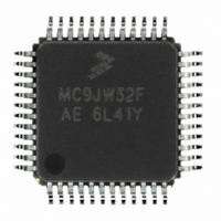
MCHC908JW32FAE Freescale Semiconductor, MCHC908JW32FAE Datasheet - Page 145

MCHC908JW32FAE
Manufacturer Part Number
MCHC908JW32FAE
Description
IC MCU 32K FLASH 8MHZ 48-LQFP
Manufacturer
Freescale Semiconductor
Series
HC08r
Datasheet
1.RD3152MMA7260Q.pdf
(232 pages)
Specifications of MCHC908JW32FAE
Core Processor
HC08
Core Size
8-Bit
Speed
8MHz
Connectivity
SPI, USB
Peripherals
LED, LVD, POR, PWM
Number Of I /o
29
Program Memory Size
32KB (32K x 8)
Program Memory Type
FLASH
Ram Size
1K x 8
Voltage - Supply (vcc/vdd)
3.5 V ~ 5.5 V
Oscillator Type
Internal
Operating Temperature
0°C ~ 70°C
Package / Case
48-LQFP
Controller Family/series
HC08
No. Of I/o's
48
Ram Memory Size
1KB
Cpu Speed
8MHz
No. Of Timers
1
Embedded Interface Type
SPI
Rohs Compliant
Yes
Processor Series
HC08JW
Core
HC08
Data Bus Width
8 bit
Data Ram Size
1 KB
Interface Type
SPI, USB
Number Of Programmable I/os
29
Number Of Timers
2
Maximum Operating Temperature
+ 70 C
Mounting Style
SMD/SMT
Development Tools By Supplier
FSICEBASE, DEMO908GZ60E, M68EML08GZE, KITUSBSPIDGLEVME, KITUSBSPIEVME, KIT33810EKEVME
Minimum Operating Temperature
0 C
Lead Free Status / RoHS Status
Lead free / RoHS Compliant
Eeprom Size
-
Data Converters
-
Lead Free Status / Rohs Status
Details
Available stocks
Company
Part Number
Manufacturer
Quantity
Price
Company:
Part Number:
MCHC908JW32FAE
Manufacturer:
Freescale Semiconductor
Quantity:
10 000
Part Number:
MCHC908JW32FAE
Manufacturer:
FREESCALE
Quantity:
20 000
- Current page: 145 of 232
- Download datasheet (3Mb)
SPR1 and SPR0 — SPI Baud Rate Select Bits
Use this formula to calculate the SPI baud rate:
where:
10.13.3 SPI Data Register
The SPI data register consists of the read-only receive data register and the write-only transmit data
register. Writing to the SPI data register writes data into the transmit data register. Reading the SPI data
register reads data from the receive data register. The transmit data and receive data registers are
separate registers that can contain different values. (See
R7–R0/T7–T0 — Receive/Transmit Data Bits
Freescale Semiconductor
In master mode, these read/write bits select one of four baud rates as shown in
SPR0 have no effect in slave mode. Reset clears SPR1 and SPR0.
CGMOUT = base clock output of the clock generator module (CGM)
BD = baud rate divisor
Address:
Do not use read-modify-write instructions on the SPI data register since the
register read is not the same as the register written.
Reset:
Read:
Write:
SPR1 and SPR0
$004E
Bit 7
R7
T7
00
01
10
11
Baud rate
Table 10-4. SPI Master Baud Rate Selection
Figure 10-15. SPI Data Register (SPDR)
R6
T6
6
MC68HC908JW32 Data Sheet, Rev. 6
=
CGMOUT
------------------------- -
2 BD
R5
T5
5
×
NOTE
Unaffected by reset
R4
T4
4
Baud Rate Divisor (BD)
Figure
R3
T3
3
128
32
10-2.)
2
8
R2
T2
2
R1
T1
1
Table
Bit 0
R0
T0
10-4. SPR1 and
I/O Registers
145
Related parts for MCHC908JW32FAE
Image
Part Number
Description
Manufacturer
Datasheet
Request
R
Part Number:
Description:
Manufacturer:
Freescale Semiconductor, Inc
Datasheet:
Part Number:
Description:
Manufacturer:
Freescale Semiconductor, Inc
Datasheet:
Part Number:
Description:
Manufacturer:
Freescale Semiconductor, Inc
Datasheet:
Part Number:
Description:
Manufacturer:
Freescale Semiconductor, Inc
Datasheet:
Part Number:
Description:
Manufacturer:
Freescale Semiconductor, Inc
Datasheet:
Part Number:
Description:
Manufacturer:
Freescale Semiconductor, Inc
Datasheet:
Part Number:
Description:
Manufacturer:
Freescale Semiconductor, Inc
Datasheet:
Part Number:
Description:
Manufacturer:
Freescale Semiconductor, Inc
Datasheet:
Part Number:
Description:
Manufacturer:
Freescale Semiconductor, Inc
Datasheet:
Part Number:
Description:
Manufacturer:
Freescale Semiconductor, Inc
Datasheet:
Part Number:
Description:
Manufacturer:
Freescale Semiconductor, Inc
Datasheet:
Part Number:
Description:
Manufacturer:
Freescale Semiconductor, Inc
Datasheet:
Part Number:
Description:
Manufacturer:
Freescale Semiconductor, Inc
Datasheet:
Part Number:
Description:
Manufacturer:
Freescale Semiconductor, Inc
Datasheet:
Part Number:
Description:
Manufacturer:
Freescale Semiconductor, Inc
Datasheet:


