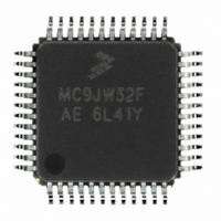
MCHC908JW32FAE Freescale Semiconductor, MCHC908JW32FAE Datasheet - Page 109

MCHC908JW32FAE
Manufacturer Part Number
MCHC908JW32FAE
Description
IC MCU 32K FLASH 8MHZ 48-LQFP
Manufacturer
Freescale Semiconductor
Series
HC08r
Datasheet
1.RD3152MMA7260Q.pdf
(232 pages)
Specifications of MCHC908JW32FAE
Core Processor
HC08
Core Size
8-Bit
Speed
8MHz
Connectivity
SPI, USB
Peripherals
LED, LVD, POR, PWM
Number Of I /o
29
Program Memory Size
32KB (32K x 8)
Program Memory Type
FLASH
Ram Size
1K x 8
Voltage - Supply (vcc/vdd)
3.5 V ~ 5.5 V
Oscillator Type
Internal
Operating Temperature
0°C ~ 70°C
Package / Case
48-LQFP
Controller Family/series
HC08
No. Of I/o's
48
Ram Memory Size
1KB
Cpu Speed
8MHz
No. Of Timers
1
Embedded Interface Type
SPI
Rohs Compliant
Yes
Processor Series
HC08JW
Core
HC08
Data Bus Width
8 bit
Data Ram Size
1 KB
Interface Type
SPI, USB
Number Of Programmable I/os
29
Number Of Timers
2
Maximum Operating Temperature
+ 70 C
Mounting Style
SMD/SMT
Development Tools By Supplier
FSICEBASE, DEMO908GZ60E, M68EML08GZE, KITUSBSPIDGLEVME, KITUSBSPIEVME, KIT33810EKEVME
Minimum Operating Temperature
0 C
Lead Free Status / RoHS Status
Lead free / RoHS Compliant
Eeprom Size
-
Data Converters
-
Lead Free Status / Rohs Status
Details
Available stocks
Company
Part Number
Manufacturer
Quantity
Price
Company:
Part Number:
MCHC908JW32FAE
Manufacturer:
Freescale Semiconductor
Quantity:
10 000
Part Number:
MCHC908JW32FAE
Manufacturer:
FREESCALE
Quantity:
20 000
8.4.1 TIM Counter Prescaler
The TIM clock source can be one of the seven prescaler outputs or the TIM clock pin, TCLK. The
prescaler generates seven clock rates from the internal bus clock. The prescaler select bits, PS[2:0], in
the TIM status and control register select the TIM clock source.
8.4.2 Input Capture
With the input capture function, the TIM can capture the time at which an external event occurs. When an
active edge occurs on the pin of an input capture channel, the TIM latches the contents of the TIM counter
into the TIM channel registers, TCHxH:TCHxL. The polarity of the active edge is programmable. Input
captures can generate TIM CPU interrupt requests.
Freescale Semiconductor
$000A
$000C
$000D
$000E
$000F
$0010
$0011
$0012
$0013
$0014
$0015
Addr.
Timer 1 Channel 0 Status and
Timer 1 Channel 1 Status and
Timer 1 Status and Control
Control Register (T1SC0)
Control Register (T1SC1)
Timer 1 Counter Modulo
Timer 1 Counter Modulo
Register Name
Timer 1 Channel 0
Timer 1 Channel 0
Timer 1 Channel 1
Timer 1 Channel 1
Timer 1 Counter
Timer 1 Counter
Register High
Register High
Register Low
Register High
Register High
Register Low
Register Low
Register Low
(T1MODH)
(T1MODL)
(T1CNTH)
(T1CH0H)
(T1CH1H)
(T1CNTL)
(T1CH0L)
(T1CH1L)
Register
(T1SC)
Reset:
Reset:
Reset:
Reset:
Reset:
Reset:
Reset:
Reset:
Reset:
Reset:
Reset:
Read:
Read:
Read:
Read:
Read:
Read:
Read:
Read:
Read:
Read:
Read:
Write:
Write:
Write:
Write:
Write:
Write:
Write:
Write:
Write:
Write:
Write:
Figure 8-2. TIM I/O Register Summary
CH1F
Bit 15
Bit 15
CH0F
Bit 15
Bit 15
Bit 7
TOF
Bit 7
Bit 7
Bit 7
Bit 7
MC68HC908JW32 Data Sheet, Rev. 6
0
0
0
0
1
1
0
0
0
0
= Unimplemented
CH0IE
CH1IE
TOIE
14
14
14
14
6
0
0
6
0
1
6
1
0
6
0
6
TSTOP
MS0B
13
13
13
13
5
1
0
5
0
1
5
1
0
5
0
0
5
Indeterminate after reset
Indeterminate after reset
Indeterminate after reset
Indeterminate after reset
TRST
MS0A
MS1A
12
12
12
12
4
0
0
0
4
0
1
4
1
0
4
0
4
ELS0B
ELS1B
11
11
11
11
3
0
0
0
3
0
1
3
1
0
3
0
3
ELS0A
ELS1A
PS2
10
10
10
10
2
0
0
2
0
1
2
1
0
2
0
2
Functional Description
TOV0
TOV1
PS1
1
0
9
0
1
0
9
1
1
1
0
9
1
0
9
1
CH0MAX
CH1MAX
Bit 0
PS0
Bit 8
Bit 0
Bit 8
Bit 0
Bit 8
Bit 0
Bit 8
Bit 0
0
0
0
1
1
0
0
109


