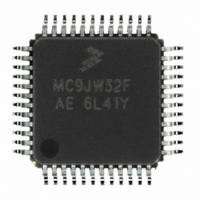
MCHC908JW32FAE Freescale Semiconductor, MCHC908JW32FAE Datasheet - Page 62

MCHC908JW32FAE
Manufacturer Part Number
MCHC908JW32FAE
Description
IC MCU 32K FLASH 8MHZ 48-LQFP
Manufacturer
Freescale Semiconductor
Series
HC08r
Datasheet
1.RD3152MMA7260Q.pdf
(232 pages)
Specifications of MCHC908JW32FAE
Core Processor
HC08
Core Size
8-Bit
Speed
8MHz
Connectivity
SPI, USB
Peripherals
LED, LVD, POR, PWM
Number Of I /o
29
Program Memory Size
32KB (32K x 8)
Program Memory Type
FLASH
Ram Size
1K x 8
Voltage - Supply (vcc/vdd)
3.5 V ~ 5.5 V
Oscillator Type
Internal
Operating Temperature
0°C ~ 70°C
Package / Case
48-LQFP
Controller Family/series
HC08
No. Of I/o's
48
Ram Memory Size
1KB
Cpu Speed
8MHz
No. Of Timers
1
Embedded Interface Type
SPI
Rohs Compliant
Yes
Processor Series
HC08JW
Core
HC08
Data Bus Width
8 bit
Data Ram Size
1 KB
Interface Type
SPI, USB
Number Of Programmable I/os
29
Number Of Timers
2
Maximum Operating Temperature
+ 70 C
Mounting Style
SMD/SMT
Development Tools By Supplier
FSICEBASE, DEMO908GZ60E, M68EML08GZE, KITUSBSPIDGLEVME, KITUSBSPIEVME, KIT33810EKEVME
Minimum Operating Temperature
0 C
Lead Free Status / RoHS Status
Lead free / RoHS Compliant
Eeprom Size
-
Data Converters
-
Lead Free Status / Rohs Status
Details
Available stocks
Company
Part Number
Manufacturer
Quantity
Price
Company:
Part Number:
MCHC908JW32FAE
Manufacturer:
Freescale Semiconductor
Quantity:
10 000
Part Number:
MCHC908JW32FAE
Manufacturer:
FREESCALE
Quantity:
20 000
Clock Generator Module (CGM)
The following conditions apply when in manual mode:
5.3.6 Programming the PLL
The following procedure shows how to program the PLL.
62
1. Choose the desired bus frequency, f
2. Choose a practical PLL reference frequency, f
•
•
•
•
•
ACQ is a writable control bit that controls the mode of the filter. Before turning on the PLL in manual
mode, the ACQ bit must be clear.
Before entering tracking mode (ACQ = 1), software must wait a given time, t
Acquisition/Lock Time
control register (PCTL).
Software must wait a given time, t
clock source to CGMOUT (BCS = 1).
The LOCK bit is disabled.
CPU interrupts from the CGM are disabled.
solve for the other.
The relationship between f
the reference is 4MHz and R = 1.
Frequency errors to the PLL are corrected at a rate of f
this rate must be as fast as possible. The VCO frequency must be an integer multiple of this rate.
The relationship between the VCO frequency, f
where N is the integer range multiplier, between 1 and 4095.
In cases where desired bus frequency has some tolerance, choose f
either by other module requirements (such as modules which are clocked by CGMXCLK), cost
requirements, or ideally, as high as the specified range allows. See
Specifications.
Choose the reference divider, R = 1.
When the tolerance on the bus frequency is tight, choose f
and R = 1. If f
practical choices of f
The round function in the following equations means that the real number
should be rounded to the nearest integer number.
RCLK
R
cannot meet this requirement, use the following equation to solve for R with
RCLK
=
Specifications.), after turning on the PLL by setting PLLON in the PLL
round R
, and choose the f
BUS
MC68HC908JW32 Data Sheet, Rev. 6
and f
MAX
AL
, after entering tracking mode before selecting the PLL as the
×
VCLK
BUSDES
f
f
VCLK
⎧
⎨
⎩
VCLK
⎛
⎜
⎝
f
------------------------- -
VCLKDES
is governed by the equation:
f
RCLK
NOTE
=
=
RCLK
, or the desired VCO frequency, f
6
2
----------- f
RCLK
P
×
R
VCLK
N
that gives the lowest R.
⎞
⎟
⎠
f
BUS
(
–
, and the reference clock divider, R. Typically,
RCLK
integer
, and the reference frequency, f
RCLK
)
/R. For stability and lock time reduction,
RCLK
⎛
⎜
⎝
f
------------------------- -
VCLKDES
f
RCLK
to an integer divisor of f
Chapter 19 Electrical
RCLK
⎞
⎟
⎠
⎫
⎬
⎭
to a value determined
ACQ
Freescale Semiconductor
VCLKDES
(See
RCLK
5.8
; and then
BUSDES
, is
,


