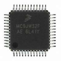
MCHC908JW32FAE Freescale Semiconductor, MCHC908JW32FAE Datasheet - Page 159

MCHC908JW32FAE
Manufacturer Part Number
MCHC908JW32FAE
Description
IC MCU 32K FLASH 8MHZ 48-LQFP
Manufacturer
Freescale Semiconductor
Series
HC08r
Datasheet
1.RD3152MMA7260Q.pdf
(232 pages)
Specifications of MCHC908JW32FAE
Core Processor
HC08
Core Size
8-Bit
Speed
8MHz
Connectivity
SPI, USB
Peripherals
LED, LVD, POR, PWM
Number Of I /o
29
Program Memory Size
32KB (32K x 8)
Program Memory Type
FLASH
Ram Size
1K x 8
Voltage - Supply (vcc/vdd)
3.5 V ~ 5.5 V
Oscillator Type
Internal
Operating Temperature
0°C ~ 70°C
Package / Case
48-LQFP
Controller Family/series
HC08
No. Of I/o's
48
Ram Memory Size
1KB
Cpu Speed
8MHz
No. Of Timers
1
Embedded Interface Type
SPI
Rohs Compliant
Yes
Processor Series
HC08JW
Core
HC08
Data Bus Width
8 bit
Data Ram Size
1 KB
Interface Type
SPI, USB
Number Of Programmable I/os
29
Number Of Timers
2
Maximum Operating Temperature
+ 70 C
Mounting Style
SMD/SMT
Development Tools By Supplier
FSICEBASE, DEMO908GZ60E, M68EML08GZE, KITUSBSPIDGLEVME, KITUSBSPIEVME, KIT33810EKEVME
Minimum Operating Temperature
0 C
Lead Free Status / RoHS Status
Lead free / RoHS Compliant
Eeprom Size
-
Data Converters
-
Lead Free Status / Rohs Status
Details
Available stocks
Company
Part Number
Manufacturer
Quantity
Price
Company:
Part Number:
MCHC908JW32FAE
Manufacturer:
Freescale Semiconductor
Quantity:
10 000
Part Number:
MCHC908JW32FAE
Manufacturer:
FREESCALE
Quantity:
20 000
DVALID_OUT — Data valid enable bit for OUT packet
TFRC_OUT — Transfer Complete Flag for OUT packet
11.5.5 USB Endpoint 1–4 Control Status Register (UEP1CSR–UEP4CSR)
TFRC — Transfer Complete Flag
DVALID — Data valid bit
Freescale Semiconductor
This bit indicates valid data is stored in the endpoint buffer, CPU attention is required. User must clear
this bit in order to receive the next OUT packet by writing zero to the bit, otherwise all successive OUT
packet is NAK by the module. Writing one to the bit has no effect. Reset clears this bit.
This read/write bit indicates the a valid OUT or SETUP packet is completely transferred to the EP0
data buffer. When the bit is set, all successive OUT packet will be responded by NAK. Writing zero to
clear this bit. Writing one to the bit has no effect.
This read/write bit indicates the data transfer associated with the endpoint is completed. When the bit
is set, all successive IN/OUT packet will be responded by NAK. Writing zero to clear this bit. Writing
one to the bit has no effect.
When the endpoint is configured as IN endpoint, this bit indicates the data in the endpoint buffer is valid
and ready to be sent. Setting this bit arms the data transmission otherwise all IN packets are returned
by NAK. The bit will be cleared automatically by hardware when a successful IN packet transaction
occurred.
When the endpoint is configured as OUT endpoint, this bit indicates valid received data is stored in the
endpoint buffer, CPU attention is required. User must clear this bit in order to receive the next OUT
packet, otherwise all successive OUT packet is responded NAK by the module. Reset clears this bit.
1 = Data in the EP0 buffer is valid
0 = Data in the EP0 buffer is not valid
1 = Endpoint data transfer completed
0 = Default status
1 = Endpoint data transfer completed
0 = Default status
1 = Data in the endpoint buffer is valid
0 = Data in the endpoint buffer is not valid
Address:
Reset:
Read:
Write:
Figure 11-7. USB Endpoint 1–4 Control Status Register
MODE1
Bit 7
$0055 to $0058
0
MODE0
6
0
MC68HC908JW32 Data Sheet, Rev. 6
STALL
5
0
0
DIR
4
0
SIZE1
3
0
SIZE0
2
0
DVALID
1
0
USB Module Registers
TFRC
Bit 0
0
159


