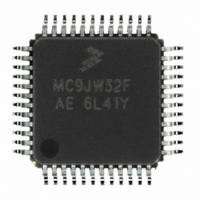
MCHC908JW32FAE Freescale Semiconductor, MCHC908JW32FAE Datasheet - Page 167

MCHC908JW32FAE
Manufacturer Part Number
MCHC908JW32FAE
Description
IC MCU 32K FLASH 8MHZ 48-LQFP
Manufacturer
Freescale Semiconductor
Series
HC08r
Datasheet
1.RD3152MMA7260Q.pdf
(232 pages)
Specifications of MCHC908JW32FAE
Core Processor
HC08
Core Size
8-Bit
Speed
8MHz
Connectivity
SPI, USB
Peripherals
LED, LVD, POR, PWM
Number Of I /o
29
Program Memory Size
32KB (32K x 8)
Program Memory Type
FLASH
Ram Size
1K x 8
Voltage - Supply (vcc/vdd)
3.5 V ~ 5.5 V
Oscillator Type
Internal
Operating Temperature
0°C ~ 70°C
Package / Case
48-LQFP
Controller Family/series
HC08
No. Of I/o's
48
Ram Memory Size
1KB
Cpu Speed
8MHz
No. Of Timers
1
Embedded Interface Type
SPI
Rohs Compliant
Yes
Processor Series
HC08JW
Core
HC08
Data Bus Width
8 bit
Data Ram Size
1 KB
Interface Type
SPI, USB
Number Of Programmable I/os
29
Number Of Timers
2
Maximum Operating Temperature
+ 70 C
Mounting Style
SMD/SMT
Development Tools By Supplier
FSICEBASE, DEMO908GZ60E, M68EML08GZE, KITUSBSPIDGLEVME, KITUSBSPIEVME, KIT33810EKEVME
Minimum Operating Temperature
0 C
Lead Free Status / RoHS Status
Lead free / RoHS Compliant
Eeprom Size
-
Data Converters
-
Lead Free Status / Rohs Status
Details
Available stocks
Company
Part Number
Manufacturer
Quantity
Price
Company:
Part Number:
MCHC908JW32FAE
Manufacturer:
Freescale Semiconductor
Quantity:
10 000
Part Number:
MCHC908JW32FAE
Manufacturer:
FREESCALE
Quantity:
20 000
Chapter 13
Input/Output (I/O) Ports
13.1 Introduction
Twenty-nine (34) bidirectional input-output (I/O) pins form five parallel ports. All I/O pins are
programmable as inputs or outputs.
Input pins and I/O port pins that are not used in the application must be terminated. This prevents excess
current caused by floating inputs, and enhances immunity during noise or transient events. Termination
methods include:
Never connect unused pins directly to V
Since some general-purpose I/O pins are not available on all packages, these pins must be terminated
as well. Either method 1 or 2 above are appropriate.
Freescale Semiconductor
$0000
$0001
$0002
$0003
$0008
$0004
Addr.
1. Configuring unused pins as outputs and driving high or low;
2. Configuring unused pins as inputs and enabling internal pull-ups;
3. Configuring unused pins as inputs and using external pull-up or pull-down resistors.
Data Direction Register A
Register Name
Port C Data Register
Port D Data Register
Port A Data Register
Port B Data Register
Port E Data Register
(DDRA)
(PTA)
(PTB)
(PTC)
(PTD)
(PTE)
Reset:
Reset:
Reset:
Reset:
Reset:
Reset:
Read:
Read:
Read:
Read:
Read:
Read:
Write:
Write:
Write:
Write:
Write:
Write:
Figure 13-1. I/O Port Register Summary
DDRA7
PTA7
PTB7
PTD7
PTE7
Bit 7
MC68HC908JW32 Data Sheet, Rev. 6
0
DD
= Unimplemented
or V
DDRA6
PTA6
PTB6
PTD6
PTE6
6
0
SS
.
DDRA5
PTA5
PTB5
PTD5
PTE5
5
0
DDRA4
Unaffected by reset
Unaffected by reset
Unaffected by reset
Unaffected by reset
Unaffected by reset
PTA4
PTB4
PTD4
PTE4
4
0
DDRA3
PTA3
PTB3
PTC3
PTD3
PTE3
3
0
DDRA2
PTC2
PTD2
PTA2
PTB2
PTE2
2
0
DDRA1
PTC1
PTD1
PTA1
PTB1
1
0
DDRA0
PTC0
PTD0
PTA0
PTB0
Bit 0
0
167


