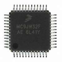
MCHC908JW32FAE Freescale Semiconductor, MCHC908JW32FAE Datasheet - Page 140

MCHC908JW32FAE
Manufacturer Part Number
MCHC908JW32FAE
Description
IC MCU 32K FLASH 8MHZ 48-LQFP
Manufacturer
Freescale Semiconductor
Series
HC08r
Datasheet
1.RD3152MMA7260Q.pdf
(232 pages)
Specifications of MCHC908JW32FAE
Core Processor
HC08
Core Size
8-Bit
Speed
8MHz
Connectivity
SPI, USB
Peripherals
LED, LVD, POR, PWM
Number Of I /o
29
Program Memory Size
32KB (32K x 8)
Program Memory Type
FLASH
Ram Size
1K x 8
Voltage - Supply (vcc/vdd)
3.5 V ~ 5.5 V
Oscillator Type
Internal
Operating Temperature
0°C ~ 70°C
Package / Case
48-LQFP
Controller Family/series
HC08
No. Of I/o's
48
Ram Memory Size
1KB
Cpu Speed
8MHz
No. Of Timers
1
Embedded Interface Type
SPI
Rohs Compliant
Yes
Processor Series
HC08JW
Core
HC08
Data Bus Width
8 bit
Data Ram Size
1 KB
Interface Type
SPI, USB
Number Of Programmable I/os
29
Number Of Timers
2
Maximum Operating Temperature
+ 70 C
Mounting Style
SMD/SMT
Development Tools By Supplier
FSICEBASE, DEMO908GZ60E, M68EML08GZE, KITUSBSPIDGLEVME, KITUSBSPIEVME, KIT33810EKEVME
Minimum Operating Temperature
0 C
Lead Free Status / RoHS Status
Lead free / RoHS Compliant
Eeprom Size
-
Data Converters
-
Lead Free Status / Rohs Status
Details
Available stocks
Company
Part Number
Manufacturer
Quantity
Price
Company:
Part Number:
MCHC908JW32FAE
Manufacturer:
Freescale Semiconductor
Quantity:
10 000
Part Number:
MCHC908JW32FAE
Manufacturer:
FREESCALE
Quantity:
20 000
Serial Peripheral Interface Module (SPI)
To protect status bits during the break state, write a logic 0 to the BCFE bit. With BCFE at logic 0 (its
default state), software can read and write I/O registers during the break state without affecting status bits.
Some status bits have a 2-step read/write clearing procedure. If software does the first step on such a bit
before the break, the bit cannot change during the break state as long as BCFE is at logic 0. After the
break, doing the second step clears the status bit.
Since the SPTE bit cannot be cleared during a break with the BCFE bit cleared, a write to the transmit
data register in break mode does not initiate a transmission nor is this data transferred into the shift
register. Therefore, a write to the SPDR in break mode with the BCFE bit cleared has no effect.
10.12 I/O Signals
The SPI module has five I/O pins and shares four of them with a parallel I/O port. They are:
The SPI has limited inter-integrated circuit (I
single-master environment. To communicate with I
when the SPWOM bit in the SPI control register is set. In I
are connected to a bidirectional pin from the I
10.12.1 MISO (Master In/Slave Out)
MISO is one of the two SPI module pins that transmits serial data. In full duplex operation, the MISO pin
of the master SPI module is connected to the MISO pin of the slave SPI module. The master SPI
simultaneously receives data on its MISO pin and transmits data from its MOSI pin.
Slave output data on the MISO pin is enabled only when the SPI is configured as a slave. The SPI is
configured as a slave when its SPMSTR bit is logic 0 and its SS pin is at logic 0. To support a
multiple-slave system, a logic 1 on the SS pin puts the MISO pin in a high-impedance state.
When enabled, the SPI controls data direction of the MISO pin regardless of the state of the data direction
register of the shared I/O port.
10.12.2 MOSI (Master Out/Slave In)
MOSI is one of the two SPI module pins that transmits serial data. In full-duplex operation, the MOSI pin
of the master SPI module is connected to the MOSI pin of the slave SPI module. The master SPI
simultaneously transmits data from its MOSI pin and receives data on its MISO pin.
When enabled, the SPI controls data direction of the MOSI pin regardless of the state of the data direction
register of the shared I/O port.
10.12.3 SPSCK (Serial Clock)
The serial clock synchronizes data transmission between master and slave devices. In a master MCU,
the SPSCK pin is the clock output. In a slave MCU, the SPSCK pin is the clock input. In full-duplex
operation, the master and slave MCUs exchange a byte of data in eight serial clock cycles.
140
•
•
•
•
•
MISO — Data received
MOSI — Data transmitted
SPSCK — Serial clock
SS — Slave select
CGND — Clock ground (internally connected to V
MC68HC908JW32 Data Sheet, Rev. 6
2
C) capability (requiring software support) as a master in a
2
C peripheral and through a pullup resistor to V
2
C peripherals, MOSI becomes an open-drain output
SS
2
)
C communication, the MOSI and MISO pins
Freescale Semiconductor
DD
.


