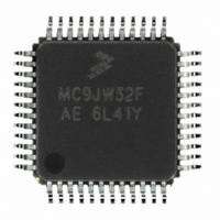
MCHC908JW32FAE Freescale Semiconductor, MCHC908JW32FAE Datasheet - Page 64

MCHC908JW32FAE
Manufacturer Part Number
MCHC908JW32FAE
Description
IC MCU 32K FLASH 8MHZ 48-LQFP
Manufacturer
Freescale Semiconductor
Series
HC08r
Datasheet
1.RD3152MMA7260Q.pdf
(232 pages)
Specifications of MCHC908JW32FAE
Core Processor
HC08
Core Size
8-Bit
Speed
8MHz
Connectivity
SPI, USB
Peripherals
LED, LVD, POR, PWM
Number Of I /o
29
Program Memory Size
32KB (32K x 8)
Program Memory Type
FLASH
Ram Size
1K x 8
Voltage - Supply (vcc/vdd)
3.5 V ~ 5.5 V
Oscillator Type
Internal
Operating Temperature
0°C ~ 70°C
Package / Case
48-LQFP
Controller Family/series
HC08
No. Of I/o's
48
Ram Memory Size
1KB
Cpu Speed
8MHz
No. Of Timers
1
Embedded Interface Type
SPI
Rohs Compliant
Yes
Processor Series
HC08JW
Core
HC08
Data Bus Width
8 bit
Data Ram Size
1 KB
Interface Type
SPI, USB
Number Of Programmable I/os
29
Number Of Timers
2
Maximum Operating Temperature
+ 70 C
Mounting Style
SMD/SMT
Development Tools By Supplier
FSICEBASE, DEMO908GZ60E, M68EML08GZE, KITUSBSPIDGLEVME, KITUSBSPIEVME, KIT33810EKEVME
Minimum Operating Temperature
0 C
Lead Free Status / RoHS Status
Lead free / RoHS Compliant
Eeprom Size
-
Data Converters
-
Lead Free Status / Rohs Status
Details
Available stocks
Company
Part Number
Manufacturer
Quantity
Price
Company:
Part Number:
MCHC908JW32FAE
Manufacturer:
Freescale Semiconductor
Quantity:
10 000
Part Number:
MCHC908JW32FAE
Manufacturer:
FREESCALE
Quantity:
20 000
Clock Generator Module (CGM)
Table 5-1
5.3.7 Special Programming Exceptions
The programming method described in
exceptions. A value of 0 for R, N, or L is meaningless when used in the equations given. To account for
these exceptions:
See
5.3.8 Base Clock Selector Circuit
This circuit is used to select either the oscillator clock, CGMXCLK, or the VCO clock, CGMVCLK, as the
source of the base clock, CGMOUT. The CGMXCLK clock is divided by two while the CGMVCLK is
divided by three to correct the duty cycle. The two divided clocks go through a transition control circuit
that to change from one clock source to the other. During this time, CGMOUT is held in stasis. Therefore,
the bus clock frequency, which is one-half of the base clock frequency, is either one-fourth the frequency
of the selected clock (CGMXCLK) or one-sixth the frequency of the selected CGMVCLK clock.
The BCS bit in the PLL control register (PCTL) selects which clock drives CGMOUT. The divided VCO
clock cannot be selected as the base clock source if the PLL is not turned on. The PLL cannot be turned
off if the divided VCO clock is selected. The PLL cannot be turned on or off simultaneously with the
selection or deselection of the divided VCO clock. The divided VCO clock also cannot be selected as the
base clock source if the factor L is programmed to a 0. This value would set up a condition inconsistent
with the operation of the PLL, so that the PLL would be disabled and the oscillator clock would be forced
as the source of the base clock.
64
9. Program the PLL registers accordingly:
•
•
5.3.8 Base Clock Selector
A 0 value for R or N is interpreted exactly the same as a value of 1.
A 0 value for L disables the PLL and prevents its selection as the source for the base clock.
a. In the PRE bits of the PLL control register (PCTL), program the binary equivalent of P.
b. In the VPR bits of the PLL control register (PCTL), program the binary equivalent of E.
d. In the PLL VCO range select register (PMRS), program the binary coded equivalent of L.
e. In the PLL reference divider select register (PMDS), program the binary coded equivalent
c. In the PLL multiplier select register low (PMSL) and the PLL multiplier select register high
provides numeric examples (numbers are in hexadecimal notation):
(PMSH), program the binary equivalent of N.
of R.
CGMVCLK
48 MHz
48 MHz
The values for P, E, N, L, and R can only be programmed when the PLL is
off (PLLON = 0).
CGMPCLK
24 MHz
24 MHz
Circuit.
MC68HC908JW32 Data Sheet, Rev. 6
Table 5-1. Numeric Examples
5.3.6 Programming the PLL
8 MHz
8 MHz
f
BUS
NOTE
4 MHz
4 MHz
f
RCLK
does not account for three possible
R
1
1
0C
06
N
P
0
1
Freescale Semiconductor
E
2
2
60
60
L


