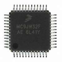
MCHC908JW32FAE Freescale Semiconductor, MCHC908JW32FAE Datasheet - Page 40

MCHC908JW32FAE
Manufacturer Part Number
MCHC908JW32FAE
Description
IC MCU 32K FLASH 8MHZ 48-LQFP
Manufacturer
Freescale Semiconductor
Series
HC08r
Datasheet
1.RD3152MMA7260Q.pdf
(232 pages)
Specifications of MCHC908JW32FAE
Core Processor
HC08
Core Size
8-Bit
Speed
8MHz
Connectivity
SPI, USB
Peripherals
LED, LVD, POR, PWM
Number Of I /o
29
Program Memory Size
32KB (32K x 8)
Program Memory Type
FLASH
Ram Size
1K x 8
Voltage - Supply (vcc/vdd)
3.5 V ~ 5.5 V
Oscillator Type
Internal
Operating Temperature
0°C ~ 70°C
Package / Case
48-LQFP
Controller Family/series
HC08
No. Of I/o's
48
Ram Memory Size
1KB
Cpu Speed
8MHz
No. Of Timers
1
Embedded Interface Type
SPI
Rohs Compliant
Yes
Processor Series
HC08JW
Core
HC08
Data Bus Width
8 bit
Data Ram Size
1 KB
Interface Type
SPI, USB
Number Of Programmable I/os
29
Number Of Timers
2
Maximum Operating Temperature
+ 70 C
Mounting Style
SMD/SMT
Development Tools By Supplier
FSICEBASE, DEMO908GZ60E, M68EML08GZE, KITUSBSPIDGLEVME, KITUSBSPIEVME, KIT33810EKEVME
Minimum Operating Temperature
0 C
Lead Free Status / RoHS Status
Lead free / RoHS Compliant
Eeprom Size
-
Data Converters
-
Lead Free Status / Rohs Status
Details
Available stocks
Company
Part Number
Manufacturer
Quantity
Price
Company:
Part Number:
MCHC908JW32FAE
Manufacturer:
Freescale Semiconductor
Quantity:
10 000
Part Number:
MCHC908JW32FAE
Manufacturer:
FREESCALE
Quantity:
20 000
Memory
2.5.7 FLASH Block Protect Register
The FLASH block protect register is implemented as an 8-bit I/O register. The value in this register
determines the starting address of the protected range within the FLASH memory.
BPR[7:0] — FLASH Block Protect Bits
40
BPR[7:1] represent bits [15:9] of a 16-bit memory address. Bits [8:0] are logic 0’s.
BPR0 is used only for BPR[7:0] = $FF, for no block protection.
The resultant 16-bit address is used for specifying the start address of the FLASH memory for block
protection. The FLASH is protected from this start address to the end of FLASH memory, at $FFFF.
With this mechanism, the protect start address can be X000, X200, etc. (at page boundaries — 512
bytes) within the FLASH memory.
Examples of protect start address:
Address:
1. The 48-byte user vectors ($FFD0–$FFFF), which are always protected.
Reset:
Read:
Write:
Start address of FLASH block protect
(0111 000x)
(0111 001x)
(0111 010x)
(1110 111x)
$EE or $EF
$70 or $71
$72 or $73
$74 or $75
BPR[7:0]
$F0 - $FF
$00–$70
$FE09
BPR7
Bit 7
0
Figure 2-5. FLASH Block Protect Register (FLBPR)
Table 2-2 FLASH Block Protect Range
BPR6
6
0
MC68HC908JW32 Data Sheet, Rev. 6
BPR5
5
0
The entire FLASH memory is NOT protected.
(The entire FLASH memory is protected.)
The entire FLASH memory is protected.
and so on...
BPR4
4
0
BPR[7:1]
Protected Range
$EE00 to $FFFF
$7000 to $FFFF
$7200 to $FFFF
$7400 to $FFFF
BPR3
3
0
16-bit memory address
BPR2
0 0 0 0 0 0 0 0 0
2
0
BPR1
1
0
(1)
Freescale Semiconductor
BPR0
Bit 0
0


