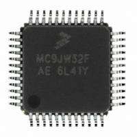
MCHC908JW32FAE Freescale Semiconductor, MCHC908JW32FAE Datasheet - Page 41

MCHC908JW32FAE
Manufacturer Part Number
MCHC908JW32FAE
Description
IC MCU 32K FLASH 8MHZ 48-LQFP
Manufacturer
Freescale Semiconductor
Series
HC08r
Datasheet
1.RD3152MMA7260Q.pdf
(232 pages)
Specifications of MCHC908JW32FAE
Core Processor
HC08
Core Size
8-Bit
Speed
8MHz
Connectivity
SPI, USB
Peripherals
LED, LVD, POR, PWM
Number Of I /o
29
Program Memory Size
32KB (32K x 8)
Program Memory Type
FLASH
Ram Size
1K x 8
Voltage - Supply (vcc/vdd)
3.5 V ~ 5.5 V
Oscillator Type
Internal
Operating Temperature
0°C ~ 70°C
Package / Case
48-LQFP
Controller Family/series
HC08
No. Of I/o's
48
Ram Memory Size
1KB
Cpu Speed
8MHz
No. Of Timers
1
Embedded Interface Type
SPI
Rohs Compliant
Yes
Processor Series
HC08JW
Core
HC08
Data Bus Width
8 bit
Data Ram Size
1 KB
Interface Type
SPI, USB
Number Of Programmable I/os
29
Number Of Timers
2
Maximum Operating Temperature
+ 70 C
Mounting Style
SMD/SMT
Development Tools By Supplier
FSICEBASE, DEMO908GZ60E, M68EML08GZE, KITUSBSPIDGLEVME, KITUSBSPIEVME, KIT33810EKEVME
Minimum Operating Temperature
0 C
Lead Free Status / RoHS Status
Lead free / RoHS Compliant
Eeprom Size
-
Data Converters
-
Lead Free Status / Rohs Status
Details
Available stocks
Company
Part Number
Manufacturer
Quantity
Price
Company:
Part Number:
MCHC908JW32FAE
Manufacturer:
Freescale Semiconductor
Quantity:
10 000
Part Number:
MCHC908JW32FAE
Manufacturer:
FREESCALE
Quantity:
20 000
Chapter 3
Configuration Registers (CONFIG)
3.1 Introduction
This section describes the configuration registers, CONFIG1 and CONFIG2. The configuration registers
enable or disable these options:
3.2 Functional Description
The configuration registers are used in the initialization of various options. The configuration register
(CONFIG1) can be written once after each reset but CONFIG2 register can perform multiple write. All of
the configuration register bits are cleared during reset. Since the various options affect the operation of
the MCU, it is recommended that these registers be written immediately after reset. The configuration
registers are located at $001D and $001F. The configuration registers may be read at anytime.
Freescale Semiconductor
† One-time writable register after each reset.
$001D
$001F
Addr.
•
•
•
•
•
•
•
•
•
Computer operating properly module (COP)
COP timeout period (262,128 or 8176 CGMRCLK cycles)
Low-voltage inhibit (LVI) module power
LVI module reset
LVI module in stop mode
LVI module voltage trip point selection
STOP instruction
Stop mode recovery time (32 CGMXCLK cycles or 4096 CGMXCLK cycles)
Oscillator during stop mode
Configuration Register 2
Configuration Register 1
Register Name
(CONFIG1)
(CONFIG2)
†
Reset:
Reset:
Read:
Read:
Write:
Write:
Figure 3-1. CONFIG Registers Summary
COPRS
Bit 7
MC68HC908JW32 Data Sheet, Rev. 6
0
0
= Unimplemented
LVISTOP
6
0
0
LVIRSTD
XCLKEN
STOP_
5
0
0
STOP_RC
LVIPWRD
CLKEN
4
0
0
3
0
0
SSREC
R
2
0
0
VREG33D
STOP
1
0
0
URSTD
COPD
Bit 0
0
0
41


