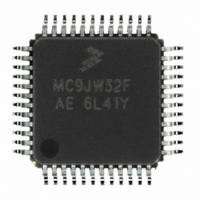
MCHC908JW32FAE Freescale Semiconductor, MCHC908JW32FAE Datasheet - Page 127

MCHC908JW32FAE
Manufacturer Part Number
MCHC908JW32FAE
Description
IC MCU 32K FLASH 8MHZ 48-LQFP
Manufacturer
Freescale Semiconductor
Series
HC08r
Datasheet
1.RD3152MMA7260Q.pdf
(232 pages)
Specifications of MCHC908JW32FAE
Core Processor
HC08
Core Size
8-Bit
Speed
8MHz
Connectivity
SPI, USB
Peripherals
LED, LVD, POR, PWM
Number Of I /o
29
Program Memory Size
32KB (32K x 8)
Program Memory Type
FLASH
Ram Size
1K x 8
Voltage - Supply (vcc/vdd)
3.5 V ~ 5.5 V
Oscillator Type
Internal
Operating Temperature
0°C ~ 70°C
Package / Case
48-LQFP
Controller Family/series
HC08
No. Of I/o's
48
Ram Memory Size
1KB
Cpu Speed
8MHz
No. Of Timers
1
Embedded Interface Type
SPI
Rohs Compliant
Yes
Processor Series
HC08JW
Core
HC08
Data Bus Width
8 bit
Data Ram Size
1 KB
Interface Type
SPI, USB
Number Of Programmable I/os
29
Number Of Timers
2
Maximum Operating Temperature
+ 70 C
Mounting Style
SMD/SMT
Development Tools By Supplier
FSICEBASE, DEMO908GZ60E, M68EML08GZE, KITUSBSPIDGLEVME, KITUSBSPIEVME, KIT33810EKEVME
Minimum Operating Temperature
0 C
Lead Free Status / RoHS Status
Lead free / RoHS Compliant
Eeprom Size
-
Data Converters
-
Lead Free Status / Rohs Status
Details
Available stocks
Company
Part Number
Manufacturer
Quantity
Price
Company:
Part Number:
MCHC908JW32FAE
Manufacturer:
Freescale Semiconductor
Quantity:
10 000
Part Number:
MCHC908JW32FAE
Manufacturer:
FREESCALE
Quantity:
20 000
Chapter 10
Serial Peripheral Interface Module (SPI)
10.1 Introduction
This section describes the serial peripheral interface (SPI) module, which allows full-duplex,
synchronous, serial communications with peripheral devices.
10.2 Features
Features of the SPI module include the following:
10.3 Pin Name Conventions and I/O Register Addresses
The text that follows describes the SPI. The SPI I/O pin names are SS (slave select), SPSCK (SPI serial
clock), CGND (clock ground), MOSI (master out slave in), and MISO (master in/slave out). The SPI
shares four I/O pins with four parallel I/O ports.
The full names of the SPI I/O pins are shown in
follows.
Figure 10-1
Freescale Semiconductor
•
•
•
•
•
•
•
•
•
•
Full-duplex operation
Master and slave modes
Double-buffered operation with separate transmit and receive registers
Four master mode frequencies (maximum = bus frequency ÷ 2)
Maximum slave mode frequency = bus frequency
Serial clock with programmable polarity and phase
Two separately enabled interrupts:
–
–
Mode fault error flag with CPU interrupt capability
Overflow error flag with CPU interrupt capability
Programmable wired-OR mode
SPRF (SPI receiver full)
SPTE (SPI transmitter empty)
summarizes the SPI I/O registers.
Pin Names:
Full SPI
SPI Generic
Pin Names:
SPI
PTE6/MISO
Table 10-1. Pin Name Conventions
MISO
MC68HC908JW32 Data Sheet, Rev. 6
PTE5/MOSI
Table
MOSI
10-1. The generic pin names appear in the text that
PTE7/SS
SS
PTE4/SPSCK
SPSCK
CGND
V
SS
127


