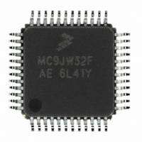
MCHC908JW32FAE Freescale Semiconductor, MCHC908JW32FAE Datasheet - Page 174

MCHC908JW32FAE
Manufacturer Part Number
MCHC908JW32FAE
Description
IC MCU 32K FLASH 8MHZ 48-LQFP
Manufacturer
Freescale Semiconductor
Series
HC08r
Datasheet
1.RD3152MMA7260Q.pdf
(232 pages)
Specifications of MCHC908JW32FAE
Core Processor
HC08
Core Size
8-Bit
Speed
8MHz
Connectivity
SPI, USB
Peripherals
LED, LVD, POR, PWM
Number Of I /o
29
Program Memory Size
32KB (32K x 8)
Program Memory Type
FLASH
Ram Size
1K x 8
Voltage - Supply (vcc/vdd)
3.5 V ~ 5.5 V
Oscillator Type
Internal
Operating Temperature
0°C ~ 70°C
Package / Case
48-LQFP
Controller Family/series
HC08
No. Of I/o's
48
Ram Memory Size
1KB
Cpu Speed
8MHz
No. Of Timers
1
Embedded Interface Type
SPI
Rohs Compliant
Yes
Processor Series
HC08JW
Core
HC08
Data Bus Width
8 bit
Data Ram Size
1 KB
Interface Type
SPI, USB
Number Of Programmable I/os
29
Number Of Timers
2
Maximum Operating Temperature
+ 70 C
Mounting Style
SMD/SMT
Development Tools By Supplier
FSICEBASE, DEMO908GZ60E, M68EML08GZE, KITUSBSPIDGLEVME, KITUSBSPIEVME, KIT33810EKEVME
Minimum Operating Temperature
0 C
Lead Free Status / RoHS Status
Lead free / RoHS Compliant
Eeprom Size
-
Data Converters
-
Lead Free Status / Rohs Status
Details
Available stocks
Company
Part Number
Manufacturer
Quantity
Price
Company:
Part Number:
MCHC908JW32FAE
Manufacturer:
Freescale Semiconductor
Quantity:
10 000
Part Number:
MCHC908JW32FAE
Manufacturer:
FREESCALE
Quantity:
20 000
Input/Output (I/O) Ports
13.4 Port C
Port C is a 4-bit general-purpose bidirectional I/O port. PTC[3:0] are shared with Timer.
13.4.1 Port C Data Register
The port C data register contains a data latch for each of the seven port C pins.
Table 13-4
PTC[3:0] — Port C Data Bits
T1CH0, T1CH1 — Timer Channels I/O Bits
TCLK1 — Timer Clock Input
174
These read/write bits are software-programmable. Data direction of each port C pin is under the control
of the corresponding bit in data direction register C. Reset has no effect on port C data.
The PTC0/T1CH0, PTC2/T1CH1 pins are the TIM input capture/output compare pins. The edge/level
select bits, ELSxB and ELSxA, determine whether they are timer channel I/O pins or general-purpose
I/O pins.
The PTC1/TCLK1 pin are the external clock input for the TIM. The prescaler select bits, PS[2:0], select
PTC1/TCLK1 as the TIM clock input. When not selected as the TIM clock, they are available for
general purpose I/O.
shows the port function priority table.
(see Chapter 8 Timer Interface Module
Additional
Function:
Address:
Data direction register C (DDRC) does not affect the data direction of port
C pins that are being used by the TIM. However, the DDRC bits always
determine whether reading port C returns the states of the latches or the
states of the pins.
Reset:
Read:
Write:
$0002
Bit 7
(see Chapter 8 Timer Interface Module
= Unimplemented
MSxB:MSxA
Figure 13-8. Port C Data Register (PTC)
01/10/11
6
Table 13-4. Port C Priority Table
00
MC68HC908JW32 Data Sheet, Rev. 6
5
Timer function pins
Port logic control
NOTE
Unaffected by reset
4
(TIM))
Feature
PTC3
3
(TIM))
T1CH1
PTC2
2
T1CLK
PTC1
1
Freescale Semiconductor
T1CH0
PTC0
Bit 0


