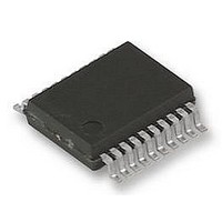
UPD78F9222MC(T)-5A4-A NEC, UPD78F9222MC(T)-5A4-A Datasheet - Page 166

UPD78F9222MC(T)-5A4-A
Manufacturer Part Number
UPD78F9222MC(T)-5A4-A
Description
8BIT MCU, 4K FLASH, 256B RAM, 78F9222
Manufacturer
NEC
Datasheet
1.UPD78F9222MCT-5A4-A.pdf
(414 pages)
Specifications of UPD78F9222MC(T)-5A4-A
Controller Family/series
UPD78
No. Of I/o's
17
Ram Memory Size
256Byte
Cpu Speed
10MHz
No. Of Timers
4
No. Of
RoHS Compliant
Core Size
8bit
Program Memory Size
4KB
Oscillator Type
External, Internal
Available stocks
Company
Part Number
Manufacturer
Quantity
Price
Company:
Part Number:
UPD78F9222MC(T)-5A4-A
Manufacturer:
NEC
Quantity:
1 000
Company:
Part Number:
UPD78F9222MC(T)-5A4-A
Manufacturer:
NEC/PBF
Quantity:
6 640
Part Number:
UPD78F9222MC(T)-5A4-A
Manufacturer:
RENESAS/瑞萨
Quantity:
20 000
- Current page: 166 of 414
- Download datasheet (4Mb)
(2) Analog input channel specification register (ADS)
(3) 10-bit A/D conversion result register (ADCR)
166
Symbol
Cautions 2. If a bit other than ADCS of ADM is manipulated while A/D conversion is stopped (ADCS = 0)
ADCR
This register specifies the input port of the analog voltage to be A/D converted.
ADS can be set by a 1-bit or 8-bit memory manipulation instruction.
Reset signal generation clears this register to 00H.
Caution Be sure to clear bits 2 to 7 of ADS to 0.
This register is a 16-bit register that stores the A/D conversion result. The higher six bits are fixed to 0. Each
time A/D conversion ends, the conversion result is loaded from the successive approximation register, and is
stored in ADCR in order starting from bit 1 of FF19H. FF19H indicates the higher 2 bits of the conversion result,
and FF18H indicates the lower 8 bits of the conversion result.
ADCR can be read by a 16-bit memory manipulation instruction.
Reset signal generation makes ADCR undefined.
Caution When writing to the A/D converter mode register (ADM) and analog input channel specification
Address: FF18H, FF19H
0
3. A/D conversion must be stopped (ADCS = 0) before rewriting bits FR0 to FR2.
4. Be sure to clear bits 6, 2, and 1 to 0.
register (ADS), the contents of ADCR may become undefined. Read the conversion result
following conversion completion before writing to ADM and ADS. Using timing other than the
above may cause an incorrect conversion result to be read.
and then A/D conversion is started, execute two NOP instructions or an instruction
equivalent to two machine cycles, and set ADCS to 1.
Figure 10-5. Format of Analog Input Channel Specification Register (ADS)
0
Symbol
Address: FF81H
Figure 10-6. Format of 10-bit A/D Conversion Result Register (ADCR)
ADS
0
ADS1
0
7
0
0
1
1
0
FF19H
After reset: Undefined
After reset: 00H
ADS0
0
0
6
0
1
0
1
CHAPTER 10 A/D CONVERTER
User’s Manual U16898EJ5V0UD
0
ANI0
ANI1
ANI2
ANI3
0
5
Analog input channel specification
R/W
0
4
R
0
3
0
2
ADS1
1
FF18H
ADS0
0
Related parts for UPD78F9222MC(T)-5A4-A
Image
Part Number
Description
Manufacturer
Datasheet
Request
R

Part Number:
Description:
16/8 bit single-chip microcomputer
Manufacturer:
NEC
Datasheet:

Part Number:
Description:
Dual audio power amp circuit
Manufacturer:
NEC
Datasheet:

Part Number:
Description:
Dual comparator
Manufacturer:
NEC
Datasheet:

Part Number:
Description:
MOS type composite field effect transistor
Manufacturer:
NEC
Datasheet:

Part Number:
Description:
50 V/100 mA FET array incorporating 2 N-ch MOSFETs
Manufacturer:
NEC
Datasheet:

Part Number:
Description:
6-pin small MM high-frequency double transistor
Manufacturer:
NEC
Datasheet:

Part Number:
Description:
6-pin small MM high-frequency double transistor
Manufacturer:
NEC
Datasheet:

Part Number:
Description:
6-pin small MM high-frequency double transistor
Manufacturer:
NEC
Datasheet:

Part Number:
Description:
6-pin small MM high-frequency double transistor
Manufacturer:
NEC
Datasheet:

Part Number:
Description:
Twin transistors equipped with different model chips(6P small MM)
Manufacturer:
NEC
Datasheet:

Part Number:
Description:
Bipolar analog integrated circuit
Manufacturer:
NEC
Datasheet:


