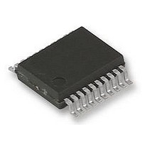
UPD78F9222MC(T)-5A4-A NEC, UPD78F9222MC(T)-5A4-A Datasheet - Page 168

UPD78F9222MC(T)-5A4-A
Manufacturer Part Number
UPD78F9222MC(T)-5A4-A
Description
8BIT MCU, 4K FLASH, 256B RAM, 78F9222
Manufacturer
NEC
Datasheet
1.UPD78F9222MCT-5A4-A.pdf
(414 pages)
Specifications of UPD78F9222MC(T)-5A4-A
Controller Family/series
UPD78
No. Of I/o's
17
Ram Memory Size
256Byte
Cpu Speed
10MHz
No. Of Timers
4
No. Of
RoHS Compliant
Core Size
8bit
Program Memory Size
4KB
Oscillator Type
External, Internal
Available stocks
Company
Part Number
Manufacturer
Quantity
Price
Company:
Part Number:
UPD78F9222MC(T)-5A4-A
Manufacturer:
NEC
Quantity:
1 000
Company:
Part Number:
UPD78F9222MC(T)-5A4-A
Manufacturer:
NEC/PBF
Quantity:
6 640
Part Number:
UPD78F9222MC(T)-5A4-A
Manufacturer:
RENESAS/瑞萨
Quantity:
20 000
- Current page: 168 of 414
- Download datasheet (4Mb)
10.4 A/D Converter Operations
10.4.1 Basic operations of A/D converter
168
<1> Set ADCE to 1.
<2> Select one channel for A/D conversion using the analog input channel specification register (ADS), and
<3> Execute two NOP instructions or an instruction equivalent to two machine cycles.
<4> Set ADCS to 1 and start the conversion operation.
<5> The voltage input to the selected analog input channel is sampled by the sample & hold circuit.
<6> When sampling has been done for a certain time, the sample & hold circuit is placed in the hold state and the
<7> Bit 9 of the successive approximation register (SAR) is set. The D/A converter voltage tap is set to (1/2)
<8> The voltage difference between the D/A converter voltage tap and analog input is compared by the voltage
<9> Next, bit 8 of SAR is automatically set to 1, and the operation proceeds to the next comparison. The D/A
<10> Comparison is continued in this way up to bit 0 of SAR.
<11> Upon completion of the comparison of 10 bits, an effective digital result value remains in SAR, and the result
<12> Repeat steps <5> to <11>, until ADCS is cleared to 0.
Cautions 1. Make sure the period of <1> to <4> is 1
Remark The following two types of A/D conversion result registers can be used.
select the conversion time using FR2 to FR0.
(<5> to <11> are operations performed by hardware.)
input analog voltage is held until the A/D conversion operation has ended.
AV
comparator. If the analog input is greater than (1/2) AV
input is smaller than (1/2) AV
converter voltage tap is selected according to the preset value of bit 9, as described below.
• Bit 9 = 1: (3/4) AV
• Bit 9 = 0: (1/4) AV
The voltage tap and analog input voltage are compared and bit 8 of SAR is manipulated as follows.
• Analog input voltage ≥ Voltage tap: Bit 8 = 1
• Analog input voltage < Voltage tap: Bit 8 = 0
value is transferred to the A/D conversion result register (ADCR, ADCRH) and then latched.
At the same time, the A/D conversion end interrupt request (INTAD) can also be generated.
To stop the A/D converter, clear ADCS to 0.
To restart A/D conversion from the status of ADCE = 1, start from <3>. To restart A/D conversion from the
status of ADCE = 0, however, start from <1> (when not changing the channel and conversion time, skip step
<2>).
REF
• ADCR (16 bits): Stores a 10-bit A/D conversion value.
• ADCRH (8 bits): Stores an 8-bit A/D conversion value.
2.
by the tap selector.
It is no problem if the order of <1> and <2> is reversed.
REF
REF
REF
, the MSB is reset to 0.
CHAPTER 10 A/D CONVERTER
User’s Manual U16898EJ5V0UD
µ
s or more.
REF
, the MSB of SAR remains set to 1. If the analog
Related parts for UPD78F9222MC(T)-5A4-A
Image
Part Number
Description
Manufacturer
Datasheet
Request
R

Part Number:
Description:
16/8 bit single-chip microcomputer
Manufacturer:
NEC
Datasheet:

Part Number:
Description:
Dual audio power amp circuit
Manufacturer:
NEC
Datasheet:

Part Number:
Description:
Dual comparator
Manufacturer:
NEC
Datasheet:

Part Number:
Description:
MOS type composite field effect transistor
Manufacturer:
NEC
Datasheet:

Part Number:
Description:
50 V/100 mA FET array incorporating 2 N-ch MOSFETs
Manufacturer:
NEC
Datasheet:

Part Number:
Description:
6-pin small MM high-frequency double transistor
Manufacturer:
NEC
Datasheet:

Part Number:
Description:
6-pin small MM high-frequency double transistor
Manufacturer:
NEC
Datasheet:

Part Number:
Description:
6-pin small MM high-frequency double transistor
Manufacturer:
NEC
Datasheet:

Part Number:
Description:
6-pin small MM high-frequency double transistor
Manufacturer:
NEC
Datasheet:

Part Number:
Description:
Twin transistors equipped with different model chips(6P small MM)
Manufacturer:
NEC
Datasheet:

Part Number:
Description:
Bipolar analog integrated circuit
Manufacturer:
NEC
Datasheet:


