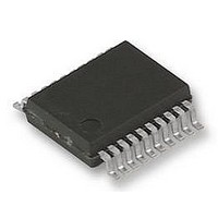
UPD78F9222MC(T)-5A4-A NEC, UPD78F9222MC(T)-5A4-A Datasheet - Page 393

UPD78F9222MC(T)-5A4-A
Manufacturer Part Number
UPD78F9222MC(T)-5A4-A
Description
8BIT MCU, 4K FLASH, 256B RAM, 78F9222
Manufacturer
NEC
Datasheet
1.UPD78F9222MCT-5A4-A.pdf
(414 pages)
Specifications of UPD78F9222MC(T)-5A4-A
Controller Family/series
UPD78
No. Of I/o's
17
Ram Memory Size
256Byte
Cpu Speed
10MHz
No. Of Timers
4
No. Of
RoHS Compliant
Core Size
8bit
Program Memory Size
4KB
Oscillator Type
External, Internal
Available stocks
Company
Part Number
Manufacturer
Quantity
Price
Company:
Part Number:
UPD78F9222MC(T)-5A4-A
Manufacturer:
NEC
Quantity:
1 000
Company:
Part Number:
UPD78F9222MC(T)-5A4-A
Manufacturer:
NEC/PBF
Quantity:
6 640
Part Number:
UPD78F9222MC(T)-5A4-A
Manufacturer:
RENESAS/瑞萨
Quantity:
20 000
- Current page: 393 of 414
- Download datasheet (4Mb)
A/D
converter
Serial
interface
UART6
Function
Interrupt
request flag
(ADIF)
Conversion
results just after
A/D conversion
start
A/D conversion
result register
(ADCR,
ADCRH) read
operation
Operating
current at
conversion
waiting mode
UART mode
RXB: Receive
buffer register 6
TXB6: Transmit
buffer register 6
Details of
Function
The interrupt request flag (ADIF) is not cleared even if the analog input channel
specification register (ADS) is changed.
Therefore, if an analog input pin is changed during A/D conversion, the A/D
conversion result and ADIF for the pre-change analog input may be set just
before the ADS rewrite. Caution is therefore required since, at this time, when
ADIF is read immediately after the ADS rewrite, ADIF is set despite the fact A/D
conversion for the post-change analog input has not ended.
When A/D conversion is stopped and then resumed, clear ADIF before the A/D
conversion operation is resumed.
The first A/D conversion value immediately after A/D conversion starts may not
fall within the rating range if the ADCS bit is set to 1 within 1
bit was set to 1, or if the ADCS bit is set to 1 with the ADCE bit = 0. Take
measures such as polling the A/D conversion end interrupt request (INTAD) and
removing the first conversion result.
When a write operation is performed to the A/D converter mode register (ADM)
and analog input channel specification register (ADS), the contents of ADCR
and ADCRH may become undefined. Read the conversion result following
conversion completion before writing to ADM and ADS. Using a timing other
than the above may cause an incorrect conversion result to be read.
The DC characteristic of the operating current during the STOP mode is not
satisfied due to the conversion waiting mode (only the comparator consumes
power), when bit 7 (ADCS) and bit 0 (ADCE) of the A/D converter mode register
(ADM) are set to 0 and 1 respectively.
The T
the reception side. To use this function, the reception side must be ready for
reception of inverted data.
If clock supply to serial interface UART6 is not stopped (e.g., in the HALT
mode), normal operation continues. If clock supply to serial interface UART6 is
stopped (e.g., in the STOP mode), each register stops operating, and holds the
value immediately before clock supply was stopped. The T
the value immediately before clock supply was stopped and outputs it.
However, the operation is not guaranteed after clock supply is resumed.
Therefore, reset the circuit so that POWER6 = 0, RXE6 = 0, and TXE6 = 0.
If data is continuously transmitted, the communication timing from the stop bit to
the next start bit is extended two operating clocks of the macro. However, this
does not affect the result of communication because the reception side
initializes the timing when it has detected a start bit. Do not use the continuous
transmission function if the interface is incorporated in LIN.
Reception enable status is entered, after having set RXE6 to 1 and one clock of
the base clock (f
When starting transmission, write transmit data to TXB6, after having set TXE6
to 1 and a wait of one clock or more of the base clock (f
performed.
Do not write data to TXB6 when bit 1 (TXBF6) of asynchronous serial interface
transmission status register 6 (ASIF6) is 1.
Do not refresh (write the same value to) TXB6 by software during a
communication operation (when bit 7 (POWER6) and bit 6 (TXE6) of
asynchronous serial interface operation mode register 6 (ASIM6) are 1 or when
bit 7 (POWER6) and bit 5 (RXE6) of ASIM6 are 1).
X
APPENDIX D LIST OF CAUTIONS
D6 output inversion function inverts only the transmission side and not
User’s Manual U16898EJ5V0UD
XCLK6
) has elapsed.
Cautions
XCLK6
X
) has been
D6 pin also holds
µ
s after the ADCE
p. 177
p. 177
p. 177
p. 179
p. 179
p. 179
p. 185
p. 185
p. 185
p. 185
p. 178
Page
(10/19)
393
Related parts for UPD78F9222MC(T)-5A4-A
Image
Part Number
Description
Manufacturer
Datasheet
Request
R

Part Number:
Description:
16/8 bit single-chip microcomputer
Manufacturer:
NEC
Datasheet:

Part Number:
Description:
Dual audio power amp circuit
Manufacturer:
NEC
Datasheet:

Part Number:
Description:
Dual comparator
Manufacturer:
NEC
Datasheet:

Part Number:
Description:
MOS type composite field effect transistor
Manufacturer:
NEC
Datasheet:

Part Number:
Description:
50 V/100 mA FET array incorporating 2 N-ch MOSFETs
Manufacturer:
NEC
Datasheet:

Part Number:
Description:
6-pin small MM high-frequency double transistor
Manufacturer:
NEC
Datasheet:

Part Number:
Description:
6-pin small MM high-frequency double transistor
Manufacturer:
NEC
Datasheet:

Part Number:
Description:
6-pin small MM high-frequency double transistor
Manufacturer:
NEC
Datasheet:

Part Number:
Description:
6-pin small MM high-frequency double transistor
Manufacturer:
NEC
Datasheet:

Part Number:
Description:
Twin transistors equipped with different model chips(6P small MM)
Manufacturer:
NEC
Datasheet:

Part Number:
Description:
Bipolar analog integrated circuit
Manufacturer:
NEC
Datasheet:


