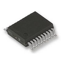
UPD78F9222MC(T)-5A4-A NEC, UPD78F9222MC(T)-5A4-A Datasheet - Page 53

UPD78F9222MC(T)-5A4-A
Manufacturer Part Number
UPD78F9222MC(T)-5A4-A
Description
8BIT MCU, 4K FLASH, 256B RAM, 78F9222
Manufacturer
NEC
Datasheet
1.UPD78F9222MCT-5A4-A.pdf
(414 pages)
Specifications of UPD78F9222MC(T)-5A4-A
Controller Family/series
UPD78
No. Of I/o's
17
Ram Memory Size
256Byte
Cpu Speed
10MHz
No. Of Timers
4
No. Of
RoHS Compliant
Core Size
8bit
Program Memory Size
4KB
Oscillator Type
External, Internal
Available stocks
Company
Part Number
Manufacturer
Quantity
Price
Company:
Part Number:
UPD78F9222MC(T)-5A4-A
Manufacturer:
NEC
Quantity:
1 000
Company:
Part Number:
UPD78F9222MC(T)-5A4-A
Manufacturer:
NEC/PBF
Quantity:
6 640
Part Number:
UPD78F9222MC(T)-5A4-A
Manufacturer:
RENESAS/瑞萨
Quantity:
20 000
- Current page: 53 of 414
- Download datasheet (4Mb)
4.2.2
output mode by using port mode register 3 (PM3). When the P30 to P31 pins are used as an input port, an on-chip
pull-up resistor can be connected in 1-bit units by using pull-up resistor option register 3 (PU3). This port is also used
for both timer I/O and external interrupt request input pin functions.
reset function. For the setting method for pin functions, see CHAPTER 17 OPTION BYTE.
Pins P30 and P31 constitute a 2-bit I/O port with an output latch. Each bit of this port can be set to the input or
Reset signal generation sets port 3 to the input mode.
P34 is a 1-bit input-only port. This pin is also used as a RESET pin, and when the power is turned on, this is the
When P34 is used as an input port pin, connect the pull-up resistor.
Figures 4-3 to 4-5 show the block diagrams of port 3.
Port 3
P3:
PU3:
PM3:
RD:
WR××: Write signal
WR
WR
WR
RD
PORT
PU
PM
Port register 3
Pull-up resistor option register 3
Port mode register 3
Read signal
Output latch
Alternate
function
PM30
PU30
(P30)
PU3
PM3
P3
Figure 4-3. Block Diagram of P30
CHAPTER 4 PORT FUNCTIONS
User’s Manual U16898EJ5V0UD
V
DD
P-ch
P30/TI000/INTP0
53
Related parts for UPD78F9222MC(T)-5A4-A
Image
Part Number
Description
Manufacturer
Datasheet
Request
R

Part Number:
Description:
16/8 bit single-chip microcomputer
Manufacturer:
NEC
Datasheet:

Part Number:
Description:
Dual audio power amp circuit
Manufacturer:
NEC
Datasheet:

Part Number:
Description:
Dual comparator
Manufacturer:
NEC
Datasheet:

Part Number:
Description:
MOS type composite field effect transistor
Manufacturer:
NEC
Datasheet:

Part Number:
Description:
50 V/100 mA FET array incorporating 2 N-ch MOSFETs
Manufacturer:
NEC
Datasheet:

Part Number:
Description:
6-pin small MM high-frequency double transistor
Manufacturer:
NEC
Datasheet:

Part Number:
Description:
6-pin small MM high-frequency double transistor
Manufacturer:
NEC
Datasheet:

Part Number:
Description:
6-pin small MM high-frequency double transistor
Manufacturer:
NEC
Datasheet:

Part Number:
Description:
6-pin small MM high-frequency double transistor
Manufacturer:
NEC
Datasheet:

Part Number:
Description:
Twin transistors equipped with different model chips(6P small MM)
Manufacturer:
NEC
Datasheet:

Part Number:
Description:
Bipolar analog integrated circuit
Manufacturer:
NEC
Datasheet:


