DO-CPLD-DK-G Xilinx Inc, DO-CPLD-DK-G Datasheet
DO-CPLD-DK-G
Specifications of DO-CPLD-DK-G
Available stocks


Related parts for DO-CPLD-DK-G


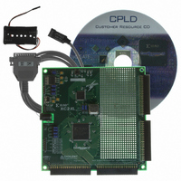
DO-CPLD-DK-G Summary of contents
Page 1
Programmable Logic Design Quick Start Handbook R ...
Page 2
... Xilinx does not assume any liability arising out of the application or use of the Design; nor does Xilinx convey any license under its patents, copyrights, or any rights of others. You are responsible for obtaining any rights you may require for your use or implementation of the Design. ...
Page 3
R About This Guide Whether you design with discrete logic, base all of your designs on microcontrollers, or simply want to learn how to use the latest and most advanced programmable logic software, you will find this book an interesting ...
Page 4
... CHAPTER 7: DESIGN REFERENCE BANK Chapter 7 contains a useful list of design examples and applications that will give you a jump start into your future programmable logic designs. This section also offers pointers on where to locate and download code and IP cores from the Xilinx website. Conventions Convention ...
Page 5
R Convention Vertical bar | Vertical ellipsis . . . Horizontal ellipsis . . . Programmable Logic Design June 12, 2006 Meaning or Use Separates items in a list of lowpwr ={on|off} choices IOB #1: Name = QOUT’ IOB #2: ...
Page 6
Preface: About This Guide vi www.xilinx.com R Programmable Logic Design June 12, 2006 ...
Page 7
Table of Contents Chapter 1:_ Introduction The History of Programmable Logic . . . . . . . . . . . . . . . . . . . . . . . . . . . . . ...
Page 8
... Before ( multiplier After ( multiplier):. . . . . . . . . . . . . . . . . . . . . . . . . . . . . . . . . . . . . . . . . . . . . . . . . . . . . . . 41 HDL Synthesis . . . . . . . . . . . . . . . . . . . . . . . . . . . . . . . . . . . . . . . . . . . . . . . . . . . . . . . . . . . . . . . . 41 ISE Software . . . . . . . . . . . . . . . . . . . . . . . . . . . . . . . . . . . . . . . . . . . . . . . . . . . . . . . . . . . . . . . . . . 41 Design Verification . . . . . . . . . . . . . . . . . . . . . . . . . . . . . . . . . . . . . . . . . . . . . . . . . . . . . . . . . . . . 42 Functional Simulation . . . . . . . . . . . . . . . . . . . . . . . . . . . . . . . . . . . . . . . . . . . . . . . . . . . . . . . . . 43 Device Implementation . . . . . . . . . . . . . . . . . . . . . . . . . . . . . . . . . . . . . . . . . . . . . . . . . . . . . . . . 44 Fitting . . . . . . . . . . . . . . . . . . . . . . . . . . . . . . . . . . . . . . . . . . . . . . . . . . . . . . . . . . . . . . . . . . . . . . . 44 Place and Route . . . . . . . . . . . . . . . . . . . . . . . . . . . . . . . . . . . . . . . . . . . . . . . . . . . . . . . . . . . . . . . 44 Downloading or Programming System Debug . . . . . . . . . . . . . . . . . . . . . . . . . . . . . . . . . . . . . . . . . . . . . . . . . . . . . . . . . . . . . . . . 46 Dynamic Verification . . . . . . . . . . . . . . . . . . . . . . . . . . . . . . . . . . . . . . . . . . . . . . . . . . . . . . . . . . 46 Debug Verification . . . . . . . . . . . . . . . . . . . . . . . . . . . . . . . . . . . . . . . . . . . . . . . . . . . . . . . . . . . . 47 Board -Level Verification . . . . . . . . . . . . . . . . . . . . . . . . . . . . . . . . . . . . . . . . . . . . . . . . . . . . . . . 47 Advanced Design Techniques Embedded SW Design Tools Center . . . . . . . . . . . . . . . . . . . . . . . . . . . . . . . . . . . . . . . . . . . . . 48 ISE WebPACK Software Registration and Installations . . . . . . . . . . . . . . . . . . . . . . . . . . . . . . . . . . . . . . . . . . . . . . . . . . . 49 Module Descriptions ...
Page 9
... Introduction . . . . . . . . . . . . . . . . . . . . . . . . . . . . . . . . . . . . . . . . . . . . . . . . . . . . . . . . . . . . . . . . . 115 CPLD Reference Designs . . . . . . . . . . . . . . . . . . . . . . . . . . . . . . . . . . . . . . . . . . . . . . . . . . . . . . 115 CoolRunner-II Application Examples . . . . . . . . . . . . . . . . . . . . . . . . . . . . . . . . . . . . . . . . . . . 117 Get the Most out of Microcontroller-Based Designs . . . . . . . . . . . . . . . . . . . . . . . . . . . . . . . 118 Design Partitioning . . . . . . . . . . . . . . . . . . . . . . . . . . . . . . . . . . . . . . . . . . . . . . . . . . . . . . . . . . . 119 Documentation and Example Code . . . . . . . . . . . . . . . . . . . . . . . . . . . . . . . . . . . . . . . . . . . . . 120 Intellectual Property (IP) Cores 120 End Markets . . . . . . . . . . . . . . . . . . . . . . . . . . . . . . . . . . . . . . . . . . . . . . . . . . . . . . . . . . . . . . . . . 121 Xilinx Design Services . . . . . . . . . . . . . . . . . . . . . . . . . . . . . . . . . . . . . . . . . . . . . . . . . . . . . . . . 121 Design Consultants . . . . . . . . . . . . . . . . . . . . . . . . . . . . . . . . . . . . . . . . . . . . . . . . . . . . . . . . . . . 122 Programmable Logic Design June 12, 2006 www ...
Page 10
Technical Support . . . . . . . . . . . . . . . . . . . . . . . . . . . . . . . . . . . . . . ...
Page 11
... Common logic shared Common logic shared Outputs do not have dedicated product terms Outputs do not have dedicated product terms Indicates ‘used’ junction Indicates ‘used’ junction Indicates ‘unused’ junction Indicates ‘unused’ junction Indicates ‘unused’ junction X X Outputs Outputs Indicates ‘ ...
Page 12
... The architecture had a mesh of horizontal and vertical interconnect tracks. At each junction was a fuse. With the aid of software tools, designers could select which junctions would not be connected by “blowing” all unwanted fuses. (This was done by a device programmer, but more commonly these days is achieved with ISP). ...
Page 13
R PLDs provide the ability to program the devices time and time again, electrically programming and erasing the device. Gone are the days of erasing for more than 20 minutes under an UV eraser. Complex Programmable Logic Devices (CPLDs) Complex ...
Page 14
... Therefore cost of ownership is dramatically reduced. Don't forget that the ease or difficulty of design changes can also affect opportunity costs. Engineers who spend time fixing old designs could be working on introducing new products and features ahead of the competition. ...
Page 15
... In 1985, Xilinx introduced a completely new idea: combine the user control and time to market of PLDs with the densities and cost benefits of gate arrays. Customers liked it, and the FPGA was born. Today Xilinx is the number one FPGA vendor in the world. An FPGA is a regular structure of logic cells (or modules) and interconnect, which is under your complete control ...
Page 16
... Chapter 1: The dominant type of FPGA is SRAM-based and can be reprogrammed as often as you choose. In fact, an SRAM FPGA is reprogrammed every time it’s powered up, because the FPGA is really a fancy memory chip. That’s why you need a serial PROM or system memory with every SRAM FPGA. In the SRAM logic cell, instead of conventional gates, an LUT determines the output based on the values of the inputs. (In the “ ...
Page 17
... The consolidation of 74 series standard logic into a low-cost CPLD is a very attractive proposition. Not only do you save PCB area and board layers – thus reducing your total system cost – but you only have to purchase and stock one generic part instead more pre-defined logic devices ...
Page 18
Chapter 1: 8 www.xilinx.com R Programmable Logic Design June 12, 2006 ...
Page 19
R Xilinx Silicon Solutions Introduction Xilinx programmable logic solutions help minimize risks for electronic equipment manufacturers by shortening the time required to develop products and take them to market. You can design and verify the unique circuits in Xilinx programmable ...
Page 20
Chapter 2: Xilinx Silicon Solutions Xilinx Devices CoolRunner-II Lowest Cost per Macrocell XC9500XL 3.3V 288 Macrocells Xilinx CPLDs Currently, Xilinx offers CPLD products in two categories: XC9500 and CoolRunner devices. This guide will focus on the two most ...
Page 21
... Low Power – Is your end product battery- or solar-powered? Does your design require the lowest power devices possible? Do you have heat dissipation concerns? System-Level Functions – Does your board have multi-voltage devices? Do you need to level shift between these devices? Do you need to square up clock edges? Do you need to interface to memories and microprocessors? CoolRunner-II Low-Power CPLDs CoolRunner -II CPLDs combine very low power with high speed, high density, and high I/O counts in a single device ...
Page 22
... By replacing conventional amplifier methods for implementing product terms (a technique that has been used in PLDs since the bipolar era) with a cascaded chain of pure CMOS gates, the dynamic power is also substantially lower than any competing CPLD ...
Page 23
R packages are surface mount, with more than half of them ball-grid technologies. The ultra- tiny packages permit maximum functional capacity in the smallest possible area. The CMOS technology used in CoolRunner-II CPLDs generates minimal heat, allowing the use of ...
Page 24
Chapter 2: Xilinx Silicon Solutions CoolRunner-II Architecture Description The CoolRunner-II CPLD is a highly uniform family of fast, low-power devices. The underlying architecture is a traditional CPLD architecture, combining macrocells into function blocks interconnected with a global routing matrix, the ...
Page 25
R The PLA is different – and better. First, any p-term can be attached to any OR gate inside the function block macrocell(s). Second, any logic function can have as many p-terms as needed attached to it within the function ...
Page 26
... Chapter 2: Xilinx Silicon Solutions either double data rate capability or the ability to distribute a slower clock (thereby saving power). For single-edge clocking or latching, either clock polarity may be selected per macrocell. CoolRunner-II macrocell details are shown in in the in figure, except the trapezoidal multiplexers have input selection from statically programmed configuration select lines (not shown) ...
Page 27
R I/O Blocks I/O blocks are primarily transceivers. However, each I/O is either automatically compliant with standard voltage ranges or can be programmed to become compliant. In addition to voltage levels, each input can selectively arrive through Schmitt-trigger inputs. This ...
Page 28
... CoolRunner-II CPLD parts. You can select which inputs to block under the control of the DataGATE function, effectively blocking controlled switching signals so that they do not drive internal chip capacitances. Output signals that do not switch are held by the bus hold feature. You can choose any set of input pins can be chosen to participate in the DataGATE function ...
Page 29
... Each macrocell has the ability to double its input clock switching frequency. shows the macrocell flip-flop with the DualEDGE option (doubled clock) at each macrocell. The source to double can be a control term clock, a product term clock, or one of the available global clocks. The ability to switch on both clock edges is vital for a number of synchronous memory interface applications as well as certain double data rate I/O applications ...
Page 30
Chapter 2: Xilinx Silicon Solutions • Four independent levels of security ♦ Hidden and scattered ♦ Affect different modes ♦ Interconnects are buried ♦ Multiple programming bits XC9500XL CPLD Overview The high-performance, low-cost XC9500XL family of Xilinx CPLDs are targeted ...
Page 31
R T (ns (ns (MHz) SYSTEM XC9500XL CPLDs also complement the higher-density Xilinx FPGAs to provide a total logic solution, within a unified development environment. The XC9500XL family is fully WebPOWERED via its free WebPACK ISE ...
Page 32
Chapter 2: Xilinx Silicon Solutions ♦ Data retention rating of 20 years ♦ Immune from "ISP Lock-Out" failure mode ♦ Allows arbitrary mixed-power sequencing and waveforms • Advanced Technology ♦ Third-generation, proven CPLD technology ♦ Mainstream, scalable, high-reliability processing ♦ ...
Page 33
R absorb many system functions, including embedded IP cores, custom system interfaces, DSP, and logic. In the car multimedia system shown in the above figure, the PCI bridge takes the form of a pre-verified drop in IP core, and the ...
Page 34
... The Spartan-3 family is based on advanced 90 nm, eight- layer metal process technology. Xilinx uses 90 nm technology to drive pricing down to under $20 for a one-million-gate FPGA (approximately 17,000 logic cells), which represents a cost savings as high as 80 percent compared to competitive offerings ...
Page 35
R The Spartan-3 FPGA memory architecture provides the optimal granularity and efficient area utilization. • Shift Register SRL16 Blocks ♦ Each CLB LUT works as a 16-bit fast, compact shift register ♦ Cascade LUTs to build longer shift registers ♦ ...
Page 36
Chapter 2: Xilinx Silicon Solutions ♦ As many as 104 multipliers support 18-bit signed or 17-bit unsigned multiplication, which you can cascade to support wider bits ♦ Constant coefficient multipliers: On-chip memories and logic cells work hand-in- ...
Page 37
R • Immunity to Temperature and Voltage Changes • Eliminates Stub Reflection • Increases System Reliability Spartan-3 Features and Benefits Table 2-4: Spartan-3 FPGA Family Overview Device System Gates Logic Cells Dedicated Multipliers Block RAM Blocks Block RAM Bits Distributed ...
Page 38
Chapter 2: Xilinx Silicon Solutions Digital clock management (DCM) Global routing resources Programmable output drive Table 2-6: Spartan-3E FPGA Family Overview Device System Gates Logic Cells Dedicated Multipliers Block RAM Blocks Block RAM Bits Distributed RAM Bits DCMs Max Differential ...
Page 39
R Spartan-3/3E System Integration Spartan-3/3E can create substantial system savings by replacing other standard system functions. $7/$2 $7/$2 Virtex FPGAs Virtex-4 FPGAs With more than 100 innovations, the Virtex-4 family represents a new milestone in the evolution of FPGA technology. ...
Page 40
... The columnar approach to building the ASMBL architecture enables Xilinx to cost- effectively develop multiple FPGA platforms, each with different combinations of feature sets. Thus, a specific platform can be optimized specifically for a certain domain of applications – such as logic, connectivity, DSP and embedded processing – to meet application requirements previously delivered only by ASICs, ASSPs and similar devices while remaining programmable at heart ...
Page 41
R Virtex-4 Variants Virtex-4 is offered in three variants; Virtex-4 LX, optimized for high performance logic functions; Virtex-4 SX, optimized for high-performance signal processing; Virtex-4 FX, optimized for embedded processing and high-speed serial connectivity. Resource Resource Resource Resource Memory Memory ...
Page 42
... Telecom, Storage, and Networking space, and other system applications requiring high-performance processing and high-bandwidth I/O. These applications can be segmented into two general application domains based on the system behavior. The embedded-processing domain is dominated by control flow operations involving complex data types. The connectivity-domain involves message- based processing and is dominated by asynchronous data flow operations ...
Page 43
... Virtex-4 SX Platform. With significantly higher DSP bandwidth at much reduced power consumption of previous Virtex-II Pro devices, the Virtex-4 SX Platform delivers the most DSP performance per dollar compared to any other device. Each DSP Slice implements an 18-bit x 18-bit MAC that can be clocked at 500MHz. The impact of Virtex-4 ...
Page 44
Chapter 2: Xilinx Silicon Solutions DSP specific enhancements to include new modes and capabilities, together with other parts of the optimized SX Platform architecture, enables more capable higher level DSP IP. 512 512 DSP DSP Slices Slices 192 192 160 ...
Page 45
R Table 2-7: Virtex-5 LX Selection Guide CLB Resources Memory Resources Clock Resources I/O Resources DSP Resources Military and Aerospace Xilinx is the leading supplier of high-reliability PLDs to the aerospace and defense markets. These devices are used in a ...
Page 46
Chapter 2: Xilinx Silicon Solutions information systems, and communications devices. To address the needs of automotive electronics designers, Xilinx has created a new family of devices with an extended industrial temperature range option. This new “XA” family consists of existing ...
Page 47
... You can use any combination of gates that you need. You must choose a specific vendor and device family library at this time, but you don’t yet have to know what device within that family you will ultimately use with respect to package and speed. ...
Page 48
Chapter 3: Xilinx Design Software 4. Generate a netlist. A netlist is a text equivalent of the circuit generated by design tools such as a schematic capture program. The netlist is a compact way for other programs to ...
Page 49
... Another inherent problem with using schematic capture is the difficulty in migrating between vendors and technologies. If you initially create your 10,000- gate design with FPGA vendor X and then want to migrate to a gate array, you would have to modify every one of those 50 pages using the gate array vendor’s component library. ...
Page 50
... HDL method is completely vendor-independent. This opens up tremendous design possibilities for engineers. To create multiplier, you could simply modify the work you’d already done for the smaller multiplier. For the schematic approach, this would entail making three copies of the 30 pages, then figuring out where to edit the 90 pages so that they addressed the larger bus widths ...
Page 51
... HDL Synthesis Once we have specified the design in a behavioral description we can convert it into gates using the process of synthesis. The synthesis tool does the intensive work of figuring out what gates to use, based on the high-level description file you provide (using schematic capture, you would have to do this manually.) Because the resulting netlist is vendor and device family-specific, you must use the appropriate vendor library ...
Page 52
... Programmable logic designs are verified by using a simulator, which is a software program that confirms the functionality or timing of a circuit. The industry-standard formats used ensure that designs can be reused vendors changes its libraries, only a synthesis recompile is necessary. Even if you decide to move to a different vendor and/or technology, you are just a compile away after selecting the new library ...
Page 53
... Programmable Logic Design June 12, 2006 Specification Libraries Schematic Synthesis Capture Netlist Verification Simulation Vectors Implementation Translate Fitting Timing Analyzer Place & Route Back-Annotation Download Device Program System Debug Printed Circuit Board Figure 3-4: The PLD Design Flow www.xilinx.com HDL Design Process HDL Test 43 ...
Page 54
... Device Implementation A design netlist completely describes the design using the gates for a specific vendor/device family. Once your design is fully verified time to place chip, a process referred to as device implementation. Translate comprises various programs used to import the design netlist and prepare it for layout ...
Page 55
... PROMs. Programming performs the same function as download, except that the configuration information is retained after the power is removed from the device. For antifuse devices, programming can only be done once per device – hence the term one- time programmable. Programming of Xilinx CPLDs can be done in-system via JTAG or with a conventional device programmer such as Data I/O. JTAG Boundary Scan – ...
Page 56
... Chapter 3: Xilinx Design Software In-system programming has an added advantage in that devices can be soldered directly to the PCB (such as TQFP surface-mount-type devices). If the design changes, the devices do not need to be removed from the board but simply re-programmed in-system. Libraries Schematic Synthesis Capture Netlist ...
Page 57
R • HDL Bencher™ • ISE Simulator • ModelSim XE • StateBench • HDL Simulation Libraries Debug Verification Debug verification tools speed up the process of viewing, identifying, and correcting design problems at different stages of the design cycle. Debug ...
Page 58
... Xilinx supplies access to specialized best-of-class tools from the embedded industry leader. This prevents you from having to embrace completely new development methodologies. You will be able to port existing legacy designs more easily to the Xilinx Platform FPGAs. ISE WebPACK Software The ISE WebPACK software, the only free downloadable design environment supported on Linux reduced feature set version of the complete ISE tool suite ...
Page 59
... CoolRunner XPLA3 XC9500/XL/XV Registration and Installation The ISE WebPACK software is available from two sources and as a download from the internet. If this book was received as part of a CoolRunner-II or Spartan-3 Design Kit, it will have been accompanied by a copy of ISE WebPACK on CD. That CD will have a Product ID that will need to be registered to generate a registration key that will enable installation ...
Page 60
... Module Descriptions In general, the design flow for FPGAs and CPLDs is very similar. Design Entry can be done in Schematic or HDL, such as VHDL, Verilog or, for CPLDs only, ABEL. The design can also comprise of a mixture of schematic diagrams and embedded HDL symbols. There is also a facility to create state machines in a diagrammatic form and let the software tools generate optimized code from a state diagram ...
Page 61
... The flow diagram below shows the similarities and differences between CPLD and FPGA software flows. When your design is complete and you are happy with the simulation results, you can then download the design to the required device. Programmable Logic Design June 12, 2006 ...
Page 62
Chapter 3: Xilinx Design Software Getting Started Licenses The MXE Simulator is the only tool that requires a license. MXE Simulator is licensed via the FlexLM product from Macrovision. It requires you to situate a starter license file on your ...
Page 63
... Enter the following into the New Project dialog box: Programmable Logic Design June 12, 2006 → Buy Online. We also show how you can convert the www.xilinx.com → → → Programs Xilinx ISE 8 Project Navigator Figure 4-1: New Project Window – Project Name www.xilinx.com Chapter 4 53 ...
Page 64
... Add a new source to the project by clicking on the New Source button. 7. Add a VHDL module and call it “Counter.” 8. Click the Next> button. 54 Figure 4-2: New Project Window – Device and Design Flow Figure 4-3: New Source Window www.xilinx.com R Programmable Logic Design June 12, 2006 ...
Page 65
... Review the contents of the final window and click the Finish button. This has automatically generated the entity in the counter VHDL module. Notice that a file called “counter.vhd” has been added to the project in the Sources in Project window of the Project Navigator. Programmable Logic Design ...
Page 66
... Window → Float in the ISE Menu. As the project builds, you will notice how the WebPACK ISE tool manages hierarchy and associated files in the Sources window. HDL Editor Double-clicking on any file name in the Sources window allows that file to be edited in the main Text Editor. The Language Template The language template is an excellent tool to assist you in creating HDL code ...
Page 67
R In this tutorial, the template uses the signal name “clk.” The design requires the signal to be called “clock.” The counter in the template is too complex for this particular requirement, so some sections are deleted. To use the ...
Page 68
... The counter module should now look like several new features are available in the Source Editor window. bar on the left side of the Source Editor window will bring up a menu of these features. can toggle the line numbers in the side bar on or off and place bookmarks to mark lines of interest in the source file ...
Page 69
... The HDL Bencher tool now reads in the design. The “Initialize Timing” box sets the frequency of the system clock, setup requirements, and output delays. The demoboard in the CPLD Design Kit has a 1.842MHz oscillator on the board. So, we shall enter a Programmable Logic Design June 12, 2006 Figure 4-8: New Source Window www.xilinx.com Functional Simulation 59 ...
Page 70
... When entering a stimulus, clicking the left mouse button on the cell will cycle through the available values for that cell. Click on the first blue box in the reset line. This will 60 Figure 4-9: Initial Timing and Clock Wizard Figure 4-10: HDL Bencher Window www.xilinx.com R Programmable Logic Design ...
Page 71
... Click the third blue box in the reset line and it will change from You have now entered a reset pulse two clock cycles in length. Save the file. The ISE Sources in Project window should look like image below simulate the test bench in the ISE Simulator, you first need to change the sources you are viewing away from those for Synthesis/Implementation to those for Behavioral Simulation ...
Page 72
... Xilinx ISE Simulator). 11. The simulation is automatically compiled by the ISE WebPACK software and when it is complete, the ISE Simulator Waveform window opens showing the result of the simulation. Click on the plus sign next to the COUNT bus so that it is possible to see all four signals that make up the bus individually ...
Page 73
... Taking a snapshot of your project saves the current state of your project in a subdirectory (with the same name as the snapshot) so that you can go back the future. You can view project snapshots by selecting the Sources window snapshot tab in the Project Navigator. If the design had only one module (one level of hierarchy), the implementation phase would be the next step ...
Page 74
... Click the Next> button, then the Finish button. The State Machine will appear. 4. Open the State Machine Wizard by clicking on the button in the main toolbar. The State Machine Wizard will appear. 64 Figure 4-16: New Source Window Figure 4-17: State Machine Wizard Window www.xilinx.com R Programmable Logic Design June 12, 2006 ...
Page 75
... Click on the Finish button and drop the state machine on the page by clicking anywhere on the page. Double-click on Reset State 0 (yellow oval). Rename the state name “RED.” Programmable Logic Design June 12, 2006 Figure 4-18: Reset Mode Dialog Box Figure 4-19) ...
Page 76
... Hit the Output Wizard button. This design will have three outputs named RD, AMB, and GRN. 10. In the DOUT field, type “RD” to declare an output. Set constant “1” with a registered output, as shown below. 11. Click on OK and then OK the Edit State box. ...
Page 77
... Hence, the traffic light completes a RED, REDAMB, GREEN, AMBER once every three cycles of the counter. 16. Finally, declare the vector TIMER by clicking on the button on the left-hand side of the toolbar. 17. Drop the marker on the page, double-click on it, and enter the name “TIMER” with a width of 4 bits (Range 3:0). Programmable Logic Design June 12, 2006 ...
Page 78
... Chapter 4: WebPACK ISE Design Entry 18. Click OK. Your completed state machine should look like this. 19. Click on the Generate HDL button on the top toolbar. 20. The Results window should read “Compiled Perfectly.” Close the dialog box and the generated HDL Browser window. 68 Figure 4-25: State Machine Drawing Figure 4-26: Compiled Results www ...
Page 79
... When you click the Close button a VHDL listed for the State Machine will open in the StateCAD HDL Browser. 22. Save and close StateCAD. Use menu items File The state diagram will be added to the top of the Sources window. (Double- clicking on this file will open up the state diagram in StateCAD.) Top-Level VHDL Designs At this point in the flow, two modules in the design are connected together by a top-level file ...
Page 80
... Chapter 4: WebPACK ISE Design Entry 1. Back up what you have done so far by taking a snapshot of the project. Use the menu bar and click Project → Take Snapshot. Select a snapshot name and click OK. 2. From the Project menu, select New Source and create a VHDL module called “ ...
Page 81
... Click on the Next> button, then the Finish button. Your new file, “top.vhd,” should look like 5. In the Sources window, highlight the “counter.vhd” module.”In the Processes window, double-click View VHDL Instantiation Template from the Design Utilities section. 6. Highlight and copy the component declaration and instantiation. ...
Page 82
... Declare a signal called “timer” by adding the following line above the component declarations inside the architecture: signal timer : std_logic_vector(3 downto 0); 72 Figure 4-34 for reference). Figure 4-34: Instantiation Template Code Added to Top File www.xilinx.com R Programmable Logic Design ...
Page 83
R 12. Connect the counter and state machine instantiated modules so that your “top.vhd” file looks like the code below. Programmable Logic Design June 12, 2006 Figure 4-35: top.vhd File www.xilinx.com Top-Level VHDL Designs 73 ...
Page 84
... It is now necessary to add in the generated VHDL into the project so that it can be implemented and simulated. Click the Libraries tab at the bottom of the sources window, expand the “work” tree, right click the file “STAT_MAC.vhd” and select properties (Source 74 Figure 4-36: Top Level Signal Connections → ...
Page 85
... Click OK to accept the changes and, when you return to the Sources tab, it should look like this: 17. Take a snapshot of the design as before (using Project → Take Snapshot…) only this time, call it “snap3” and type “VHDL top” in the comments window. Simulate the Design You can now simulate the entire design. ...
Page 86
Chapter 4: WebPACK ISE Design Entry 1. Add a new testbench waveform source as before, but this time, associate it with the module “top.” Use Project name it “Simulate_Top.” 2. The Associate Source dialog box will appear. Make sure “Top” ...
Page 87
... This section discusses the method of connecting VHDL modules via the ECS schematic tool. If you worked through the previous section, you will first need to remove the top level VHDL file top.vhd from the project this, highlight the file in the sources for Synthesis/Implementation View, right click and select Remove then click the Yes button ...
Page 88
... Chapter 4: WebPACK ISE Design Entry in the dialog box. Then remove it from the Window view by selecting the Top tab and → Window This action will take you back to the stage in the flow with only the “counter.vhd” and the “stat_mac.vhd” files. The Sources window module view should look like below ...
Page 89
... Create Schematic Symbol. 6. Returning to the Schematic editor, the symbol libraries can be found under the Symbol tab on the right hand tab in the Sources window (you may need to expand the window to get a better view). 7. Add the counter and state machine by clicking on the new library (C/Designs/Traffic) in the Categories window then selecting “ ...
Page 90
... ECS will let you decide whether to use the Autorouter or manually place the signals on the page. To add a hanging wire, click on the symbol pin to start the wire once at each vertex. Then double-click at the location where you want the wire to terminate. 11. Wire up the counter and state machine as shown below: ...
Page 91
... R 12. Select the Add Net Names tool from the Drawing toolbar. 13. Type “clock” in the Name bar of the Options tab (Processes window) and then click on the net in the schematic editor. 14. To add net names to wires that will be connected to your FPGA/CPLD I/Os, place the net name on the end of the hanging wire. Finish adding the net names “ ...
Page 92
... Marker icon is selected, the Options change. You select Add an input marker for the inputs and Add and output marker for the outputs. 17. Save the design (File → Save). Check the Sources window, Sources tab (expand the plus sign if necessary) and you will notice that the ISE software automatically recognizes that the schematic file is the top level file and reorganizes the design accordingly. Highlight “ ...
Page 93
... View HDL Functional Model. The synthesis tool actually works from this file. Note: If you want to see how the fitter does before simulation, go ahead and double-click on Implement Design in the Processes window. This will run synthesis, translation, fit the design, generate a programming file, and create translation reports, timing reports, and synthesis reports. If everything has been done correctly, green check marks will appear next to all these processes ...
Page 94
Chapter 4: WebPACK ISE Design Entry 2. Add a new testbench waveform source by right-clicking on “top_sch.sch” and selecting New Source. Select Test Bench Waveform and name this source “top_sch_tb. 3. Click Next> and then associate it with “top.” Click ...
Page 95
... Rescale Timing. Set the timing to 10000 ns to get a scale similar to above. You may have to rescale the timing again to get the scaling shown in Click File → Save to save the waveform With “top_sch_tb.tbw” selected in the Sources window (make sure Behavior Simulation view is showing),double-click Simulate Behavioral Model in the Process window. Programmable Logic Design June 12, 2006 ...
Page 96
... Chapter 4: WebPACK ISE Design Entry The Simulation will appear as follows: You are now ready the implementation stage. 86 Figure 4-55: Simulation Window www.xilinx.com R Programmable Logic Design June 12, 2006 ...
Page 97
... The steps of implementation must be carried out in this order. WebPACK ISE software will automatically perform the steps required if a particular step is selected. For example, if the design has only just been functionally simulated and you decide timing simulation, the software will automatically synthesize, translate, and fit the design. It will then generate the timing information before it opens the simulator and gives the timing simulation results ...
Page 98
... Figure 5-1: Process Window Showing Check Syntax for Counter.vhd After you have checked all the modules, highlight the top level module, then go down to the process tree and right-click on Synthesize (under Implement Design) and select Properties ...
Page 99
... Click OK in the Process Properties window and double-click on Synthesize. 7. When the synthesis is complete, a green tick will appear next to Synthesize. Double- click on View Synthesis Report. The report file (.syr) will appear in ISE. Constraints Editor To get the performance you need from a device, you must tell the implementation tools what and where performance is required. This design is particularly slow and timing constraints are unnecessary. Constraints can also be physical ...
Page 100
Chapter 5: Implementing CPLD Designs software will create a constraints file and call it “top.ucf.” It will be associated with your top level source file. Notice that the Translate step in the Implement Design section runs automatically. This is because ...
Page 101
... Process window. The UCF file will open in the main window of the ISE Project Navigator. The constraints entered into PACE can be seen in Note: If you do not see the UCF file in the Sources window, add it by using Project Source force a signal onto a global resource, you can apply the BUFG constraint. In this case, we will apply the BUFG constraint to the clock signal ...
Page 102
Chapter 5: Implementing CPLD Designs 9. The Constraints Editor will open. This tool can be used to set location constraints, but for this tutorial it will only be used to create timing constraints. 92 Figure 5-8: Pace with Global Tab ...
Page 103
... The Constraints Editor recognizes the one global signal in the design. Double- click in the Period window of the global clock signal. 11. In the Clock Period definition window, change the Time value to 10 ns. The duty cycle should stay at 50% high, 50% low. 12. Click OK. The period constraint is now written into the UCF file and can be seen in the constraints list at the bottom of the Constraints Editor ...
Page 104
Chapter 5: Implementing CPLD Designs Highlight the three outputs “red_light,” “green_light,” and “amber_light” using ctrl select. 14. In the Group Name field, type “lights” and then click the Create Group button. 15. In the Select Group box, select “lights” and ...
Page 105
... NET “clock” schmitt_trigger; The CoolRunner-II CPLD also supports different I/O standards. If the three light signals had downstream device that required the signals to conform to a certain I/O standard, you could use the following constraint syntax: NET “red_light” IOSTANDARD=LVTTL; ...
Page 106
... Implementation To implement the design, you must re-run Translate so the new constraints can be read. 1. Click on the “+” next to Implement Design in the Process window. The implementation steps are now visible. An orange question mark indicates that translate is now out of date and should be re-run. ...
Page 107
... R window. Then expand the Generate Timing branch and double-click on Timing Report. CPLD Reports Two reports are available that detail the fitting results and associated timing of the design. These are: • The Translation Report shows any errors in the design or the UCF. • ...
Page 108
... Chapter 5: Implementing CPLD Designs 3. To open the CPLD Fitter Report, expand the Fit branch and double-click on the Fitter Report process. The same information is contained in both the HTML and text reports, but the HTML report has been designed to make the information more readable and easier to find. You can browse through several sections of the HTML Fitter Report by using the menu on the left-hand side of the page ...
Page 109
... Properties → Timing Report Format → Detail. Timing Simulation The process of timing simulation is very similar to the functional method. Change the view to show sources for Post-Fit Simulation. This is done in the drop-down menu at the top of the Sources window. Programmable Logic Design ...
Page 110
... Chapter 5: Implementing CPLD Designs 4. With “top_tb.vhd” (or “top_sch_tb.vhd” for schematic flow) selected in the Sources window, expand the Xilinx ISE Simulator tree in the Process window and double- click on Simulate Post Fit Model. ISE Simulator will open, but this time implementing a different script file and compiling a post-route VHDL file (time_sim.vhd). “ ...
Page 111
... Configure Device (iMPACT) in the Process window (you may have to click the plus sign adjacent to Generate Programming File). 3. Right-click on the Xilinx XC2C256 icon that appears in the iMPACT window and select Program. The design will now download into the device. You have now successfully programmed your first CoolRunner-II CPLD. ...
Page 112
Chapter 5: Implementing CPLD Designs 102 www.xilinx.com R Programmable Logic Design June 12, 2006 ...
Page 113
R Implementing FPGA Designs Introduction Implementing an FPGA design is a slightly different process than implementing a CPLD design. The FPGA uses Map, Place and Route instead of Fit. Mapping includes tools for floorplanning and manual placing and routing. As ...
Page 114
... WebPACK ISE software will automatically perform the steps required if a particular step is selected. For example, if the design has only just been functionally simulated and you decide timing simulation, the software will automatically synthesize, map, and place and route. It will then generate the timing information before opening the simulator and giving timing simulation results. In this chapter, we’ ...
Page 115
... In the Process window, expand the Synthesis subsection by clicking on the plus sign (+) next to Synthesize. You can now check your design by double-clicking on Check Syntax. Ensure that any errors in your code are corrected before you continue. If the syntax check is OK, a green check mark will appear (as shown in ...
Page 116
... Chapter 6: Implementing FPGA Designs 3. Right-click on Synthesize - XST and select Properties. A window will appear allowing you to influence the way in which your design is interpreted. 4. Click on the HDL Options category. The FSM encoding algorithm option looks for state machines and determines the best method of optimizing. For FPGAs, state machines are usually “one-hot” encoded. This is because of the abundance of flip-flops in FPGA architectures ...
Page 117
R When synthesis chooses to use primitive macros it is known as “inference.” As registered outputs were selected in the state machine, three further registers were inferred. The Final Report section shows the resources used within the FPGA. The Constraints ...
Page 118
... CPLDs, and set pin-outs for a CoolRunner-II XC2C256-TQ144. 1. Highlight “top.ucf” in the Source window. Expand the plus sign(+) next to User Constraints and double-click Edit Constraints (Text). 2. Highlight all of the constraints (the entire file) and delete them. Save the UCF (File → ...
Page 119
... R The Constraints Editor is invoked and picks up the LOC constraints entered in PACE. These can be edited by double-clicking on them in the read-write window or under the Ports tab in the Main window. 7. With the Global tab selected right-click on the Period entry for the Clock signal. The Clock Period dialog box will appear. Enter a period of 10 ns. as shown in 8 ...
Page 120
Chapter 6: Implementing FPGA Designs 10. Highlight the three outputs “red_light,” “green_light,” and “amber_light” using ctrl select. 11. In the Group Name field, type “lights” and then click the Create Group button. 12. In the Select Group box, select lights ...
Page 121
... The UCF file should look similar to 15. Save (File → Save) and exit (File → Exit) the Xilinx Constraints Editor session. 16. Click on the plus sign “+” next to Implement Design in the Process window. 17. Implement the design by double-clicking on Implement Design (you could run each stage separately). ...
Page 122
... The Post-Map Static Timing Report shows the logic delays only (no routing) covered by the timing constraints. This design has two timing constraints, the clock period and the clock-to-out time of the three lights. If the logic-only delays don’t meet timing constraints, the additional delay added by routing will only add to the problem. ...
Page 123
... Right-click on Generate Programming File and click on Properties. 2. Under the Start-Up Options category, ensure that the FPGA Start-Up Clock is set to JTAG Clock by selecting JTAG Clock from the drop-down menu. Click OK 3. Double-click on Generate Programming File. This operation creates a .bit file that can be used by the iMPACT programmer to configure a device ...
Page 124
... The steps discussed were: • Synthesis and Synthesis Report • Timing and Physical Constraints using the Constraints Editor • The Reports Generated throughout the Implementation flow • Timing Simulation • Creating and Downloading a bitstream. 114 Figure 6-16: iMPACT www.xilinx.com R Programmable Logic Design June 12, 2006 ...
Page 125
... CPLD reference designs are HDL code-based designs that can help reduce the time of CPLD designs. They are all available free of charge. These reference designs take the form of IP, which can be used as is. Unlike purchased IP, these reference designs do not come with direct support. They are built around application notes and have been tested in WebPACK software ...
Page 126
Chapter 7: Application Notes, Reference Designs, IP, and Services http://www.origin.xilinx.com/products/silicon_solutions/cplds/resources/coolvhdlq. htm?url=/products/xaw/coolvhdlq.htm Table 7-1: Current Reference Designs Memory XAPP800: SPI Flash XAPP394: CoolRunner-II Mobile SDRAM Interface XAPP384: CoolRunner-II DDR SDRAM Interface XAPP354: NAND Interface (ABEL) XAPP354: NAND Interface (VHDL) XAPP354: NAND ...
Page 127
... Using design software, the architecture efficiently creates just the required logic to solve the problem. Unused logic remains available for future modifications, corrections or enhancement. Xilinx design software shuts down unused circuits eliminating their participation in the power consumption budget. By using gates and flip flops to build logic, CoolRunner-II CPLDs create a rich variety of diverse protocols, modulations and interfaces ...
Page 128
... CoolRunner CPLD . Get the Most out of Microcontroller-Based Designs Microcontrollers don’t make the world go round, but they most certainly help us get around in the world. You can find microcontrollers in automobiles, microwave ovens, automatic teller machines, VCRs, point-of-sale terminals, robotic devices, wireless telephones, home security systems, and satellites, to name just a few applications ...
Page 129
R instruction taking as long as three cycles – the actual speed MHz microcontroller is divided by 6. This works out to an operational speed of only 3.33 MHz. CoolRunner CPLDs are much, much faster than microcontrollers ...
Page 130
... The benefits of using an IP core include: • Faster time to market • Simplified development process • Minimal design risk • Reduced software compile time • Reduced verification time 120 → Documentation → Application Notes . www.xilinx.com Documentation List Title Generator Correction www.xilinx.com Number Family 384 CoolRunner-II 385 ...
Page 131
... R • Predictable performance/functionality. IP cores are similar to vendor-provided soft macros in that they simplify the design specification procedure by removing designers from gate-level details of commonly used functions. IP cores differ from soft macros in that they are generally much larger system- level functions, such as a PCI bus interface, DSP filter, or PCMCIA interface. They are extensively tested (and hence rarely free of charge) to prevent designers from having to verify the IP core functions themselves ...
Page 132
Chapter 7: Application Notes, Reference Designs, IP, and Services ♦ Fixed bid/fixed price contracts • FPGA Design From Specification ♦ Turnkey FPGA design, ASIC conversions, and driver development and integration ♦ Expertise in optimizing Xilinx technology to provide the best ...
Page 133
R Technical Support Xilinx provides 24-hour access to a set of sophisticated tools for resolving technical issues via the Web. The Xilinx search utility scans through thousands of answer records to return solutions for the given issue. Several problem-solver tools ...
Page 134
Chapter 7: Application Notes, Reference Designs, IP, and Services 124 www.xilinx.com R Programmable Logic Design June 12, 2006 ...
Page 135
... Back Annotation – Automatically attaching timing values to the entered design format after the design has been placed and routed in an FPGA. Behavioral Language – Top-down description from an even higher level than VHDL. Block RAM – A block bits of RAM inside an FPGA. Dual-port and synchronous operation are desirable. CAD – ...
Page 136
... DLL – Delay Locked Loop, A digital circuit used to perform clock management functions on- and off-chip. DRAM – Dynamic Random Access Memory. A low-cost/read-write memory where data is stored on capacitors and must be refreshed periodically. DRAMs are usually addressed by a sequence of two addresses – row address and column address – which makes them slower and more difficult to use than SRAMs. DSP – ...
Page 137
... ESD-protection diodes divert the current to the supply leads. 5-Volt Tolerant – Characteristic of the input or I/O pin of a 3.3V device that allows this pin to be driven to 5V without any excessive input current or device breakdown. Very desirable feature. FIFO – First-In-First-Out memory, where data is stored in the incoming sequence and is read out in the same sequence ...
Page 138
... Netlist – Textual description of logic and interconnects. See also XNF and EDIF. NRE – Non-Recurring Engineering charges. Startup cost for the creation of an ASIC, gate array, or HardWire. Pays for layout, masks, and test development. FPGAs and CPLDs do not require NRE. Optimization – Design change to improve performance. See also Synthesis. ...
Page 139
... FPGA configuration bitstream. The SPROM has a built-in address counter, receives a clock, and outputs a serial bitstream. SRAM – Static Random Access Memory. Read-write memory with data stored in latches. Faster than DRAM and with simpler timing requirements, but smaller in size and about four times as expensive than DRAM of the same capacity. SRL16 – ...
Page 140
... Mbps LVDS performance using dedicated DDR registers. TBUFs – Buffers with a tri-state option, where the output can be made inactive. Used for multiplexing different data sources onto a common bus. The pull- down-only option can use the bus as a wired AND function. ...
Page 141
... CPLD Complex Programmable Logic Device CSP Chip Scale Packaging DCI Digitally Controlled Impedance DCM Digital Clock Manager DCM Digital Control Management DES Data Encryption Standard DRAM Dynamic Random Access Memory DRC Design Rule Checker Programmable Logic Design June 12, 2006 www.xilinx.com 131 ...
Page 142
DSL Digital Subscriber Line DSP Digital Signal Processor DTV Digital Television ECS Schematic Editor EDA Electronic Design Automation EDIF Electronic Digital Interchange Format EMI Electromagnetic Interference EPROM Erasable Programmable Read Only Memory eSP emerging Standards and Protocols FAT File Allocation ...
Page 143
R LAN Local Area Network LEC Logic Equivalence Checker LMG Logic Modeling Group LSB Least Significant Bit LUT Look Up Table LVCMOS Low Voltage Complementary Metal Oxide Semiconductor LVDS Low Voltage Differential Signaling LVDSEXTLow Voltage Differential Signaling Extension LVPECL Low ...
Page 144
... Random Access Memory RC Radio Controlled ROM Read Only Memory SOP Sum of Product SPLD Simple Programmable Logic Device SRAM Static Random Access Memory SRL16 Shift Register LUT SSTL Stub Series Terminated Transceiver Logic TIM Time in Market Tpd Time of Propagation Delay (through the device) TQFP ...