DO-CPLD-DK-G Xilinx Inc, DO-CPLD-DK-G Datasheet - Page 109
DO-CPLD-DK-G
Manufacturer Part Number
DO-CPLD-DK-G
Description
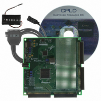
KIT DESIGN CPLD W/BATT HOLDER
Manufacturer
Xilinx Inc
Series
CoolRunner™- IIr
Type
CPLDr
Specifications of DO-CPLD-DK-G
Contents
Proto Board, Download Cable, Samples, Software
For Use With/related Products
CoolRunner-ll, XC9500XL
Lead Free Status / RoHS Status
Lead free / RoHS Compliant
Other names
122-1512
Available stocks
Company
Part Number
Manufacturer
Quantity
Price


Timing Simulation
Programmable Logic Design
June 12, 2006
R
function block (e.g., FB1) in the Function Blocks section, all of the macrocells in that
function block will be shown. Clicking on a specific macrocell will bring up a diagram of
how that macrocell is configured. An XC2C256 device has 16 function blocks, of which
only two have been used for logic functions in this design. The design could be packed into
a single function block, but the chosen I/O pins dictate which macrocells (and hence which
function blocks) are used.
A great feature of CPLDs is the deterministic timing, as a fixed delay exists per macrocell.
The Timing Report is able to give the exact propagation delays and setup times and clock-
to-out times. These values are displayed in the first section of the report you will have
created. The next section lists the longest setup time, cycle time (logic delay between
synchronous points as constrained by the period constraint), and clock-to-out time.
The setup and clock-to-out times don’t strictly affect the design’s performance. These
parameter limitations are dependent on the upstream and downstream devices on the
board. The cycle time is the maximum period of the internal system clock. The report
shows that this design has a minimum cycle time of 7.1 ns, or 140 MHz.
The next section shows all the inputs and outputs of the design and their timing
relationship with the system clock. Three lights will have a 6.0 ns delay with respect to the
clock input. The clock to setup section details the internal nets to and from a synchronous
point. The maximum delay in this section dictates the maximum system frequency.
“amber_light”, “red_light” and “green_light” are the D-Type flip-flops used to register the
outputs.
The last section details all the path type definitions, explaining the difference between the
types mentioned previously in the report.
To generate a detailed timing report, right-click on Generate Timing in the Process
window and select Properties → Timing Report Format → Detail.
The process of timing simulation is very similar to the functional method. Change the view
to show sources for Post-Fit Simulation. This is done in the drop-down menu at the
top of the Sources window.
Figure 5-16: Selecting the Post-Fit Simulation View
www.xilinx.com
Timing Simulation
99
Related parts for DO-CPLD-DK-G
Image
Part Number
Description
Manufacturer
Datasheet
Request
R

Part Number:
Description:
STARTER KIT CPLD
Manufacturer:
Xilinx Inc
Datasheet:
Part Number:
Description:
KIT STARTER CPLD JAPANESE
Manufacturer:
Xilinx Inc
Datasheet:
Part Number:
Description:
KIT STARTER CPLD-JAPANESE
Manufacturer:
Xilinx Inc
Datasheet:

Part Number:
Description:
IC CPLD .8K 36MCELL 44-VQFP
Manufacturer:
Xilinx Inc
Datasheet:

Part Number:
Description:
IC CPLD 72MCRCELL 10NS 44VQFP
Manufacturer:
Xilinx Inc
Datasheet:

Part Number:
Description:
IC CPLD 1.6K 72MCELL 64-VQFP
Manufacturer:
Xilinx Inc
Datasheet:

Part Number:
Description:
IC CR-II CPLD 64MCELL 44-VQFP
Manufacturer:
Xilinx Inc
Datasheet:

Part Number:
Description:
IC CPLD 1.6K 72MCELL 100-TQFP
Manufacturer:
Xilinx Inc
Datasheet:

Part Number:
Description:
IC CR-II CPLD 64MCELL 56-BGA
Manufacturer:
Xilinx Inc
Datasheet:

Part Number:
Description:
IC CPLD 72MCRCELL 7.5NS 44VQFP
Manufacturer:
Xilinx Inc
Datasheet:
Part Number:
Description:
IC CR-II CPLD 64MCELL 100-VQFP
Manufacturer:
Xilinx Inc
Datasheet:
Part Number:
Description:
IC CPLD 1.6K 72MCELL 100-TQFP
Manufacturer:
Xilinx Inc
Datasheet:

Part Number:
Description:
IC CPLD 72MCRCELL 7.5NS 64VQFP
Manufacturer:
Xilinx Inc
Datasheet:
Part Number:
Description:
IC CPLD 1.6K 72MCELL 100-TQFP
Manufacturer:
Xilinx Inc
Datasheet:

Part Number:
Description:
IC CPLD 1.5K 64MCELL HP 44-VQFP
Manufacturer:
Xilinx Inc