DO-CPLD-DK-G Xilinx Inc, DO-CPLD-DK-G Datasheet - Page 54
DO-CPLD-DK-G
Manufacturer Part Number
DO-CPLD-DK-G
Description
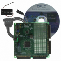
KIT DESIGN CPLD W/BATT HOLDER
Manufacturer
Xilinx Inc
Series
CoolRunner™- IIr
Type
CPLDr
Specifications of DO-CPLD-DK-G
Contents
Proto Board, Download Cable, Samples, Software
For Use With/related Products
CoolRunner-ll, XC9500XL
Lead Free Status / RoHS Status
Lead free / RoHS Compliant
Other names
122-1512
Available stocks
Company
Part Number
Manufacturer
Quantity
Price


Chapter 3: Xilinx Design Software
44
Device Implementation
Fitting
Place and Route
spend 50% of their development time going through this loop until the design works as
required.
Using HDL offers an additional advantage when verifying the design: You can simulate
directly from the HDL source file. This bypasses the time-consuming synthesis process
that would normally be required for every design change iteration. Once the circuit works
correctly, running the synthesis tool generates the netlist for the next step in the design
flow – device implementation.
A design netlist completely describes the design using the gates for a specific
vendor/device family. Once your design is fully verified, it is time to place it on a chip, a
process referred to as device implementation.
Translate comprises various programs used to import the design netlist and prepare it for
layout. The programs will vary among vendors. Some of the more common programs
during translate include: optimization, translation to the physical device elements, and
device-specific design rule checking (for example, does the design exceed the number of
clock buffers available in this device?). During this stage of the design flow, you will be
asked to select the target device, package, speed grade, and any other device-specific
options. The translate step usually ends with a comprehensive report of the results of all
the programs executed. In addition to warnings and errors is usually a listing of device and
I/O utilization, which helps you to determine if you have selected the best device.
For CPLDs, this design step is called fitting, meaning to “fit” the design to the target device.
In the diagram above, a section of the design is fit to the CPLD. CPLDs are a fixed
architecture, so the software needs to pick the gates and interconnect paths that match the
circuit. This is usually a fast process.
The biggest potential problem is if you had previously assigned the exact locations of the
I/O pins, commonly referred to as pin locking. Most often, this occurs when using a legacy
design iteration that has been committed to the printed circuit board layout. Architectures
that support I/O pin locking (such as the Xilinx XC9500 and CoolRunner CPLDs) have a
very big advantage. They allow you to keep the original I/O pin placements regardless of
the number of design changes, utilization, or required performance. Pin locking is very
important when using ISP. If you layout your PCB to accept a specific pin out, and then
change the design, you can re-program confident that you pin out will stay the same.
For FPGAs, place and route programs are run after compile. “Place” is the process of
selecting specific modules, or logic blocks, in the FPGAs where design gates will reside.
“Route,” as the name implies, is the physical routing of the interconnect between the logic
blocks. Most vendors provide automatic place and route tools so that you don’t have to
worry about the intricate details of the device architecture. Some vendors offer tools that
allow expert users to manually place and/or route the most critical parts of their designs to
achieve better performance than with the automatic tools. Floorplanner is a type of manual
tool.
Place and route programs require the longest time to complete successfully because it’s a
complex task to determine the location of large designs, ensure that they all get connected
correctly, and meet the desired performance. These programs however, can only work well
if the target architecture has sufficient routing for the design. No amount of fancy coding
www.xilinx.com
Programmable Logic Design
June 12, 2006
R
Related parts for DO-CPLD-DK-G
Image
Part Number
Description
Manufacturer
Datasheet
Request
R

Part Number:
Description:
STARTER KIT CPLD
Manufacturer:
Xilinx Inc
Datasheet:
Part Number:
Description:
KIT STARTER CPLD JAPANESE
Manufacturer:
Xilinx Inc
Datasheet:
Part Number:
Description:
KIT STARTER CPLD-JAPANESE
Manufacturer:
Xilinx Inc
Datasheet:

Part Number:
Description:
IC CPLD .8K 36MCELL 44-VQFP
Manufacturer:
Xilinx Inc
Datasheet:

Part Number:
Description:
IC CPLD 72MCRCELL 10NS 44VQFP
Manufacturer:
Xilinx Inc
Datasheet:

Part Number:
Description:
IC CPLD 1.6K 72MCELL 64-VQFP
Manufacturer:
Xilinx Inc
Datasheet:

Part Number:
Description:
IC CR-II CPLD 64MCELL 44-VQFP
Manufacturer:
Xilinx Inc
Datasheet:

Part Number:
Description:
IC CPLD 1.6K 72MCELL 100-TQFP
Manufacturer:
Xilinx Inc
Datasheet:

Part Number:
Description:
IC CR-II CPLD 64MCELL 56-BGA
Manufacturer:
Xilinx Inc
Datasheet:

Part Number:
Description:
IC CPLD 72MCRCELL 7.5NS 44VQFP
Manufacturer:
Xilinx Inc
Datasheet:
Part Number:
Description:
IC CR-II CPLD 64MCELL 100-VQFP
Manufacturer:
Xilinx Inc
Datasheet:
Part Number:
Description:
IC CPLD 1.6K 72MCELL 100-TQFP
Manufacturer:
Xilinx Inc
Datasheet:

Part Number:
Description:
IC CPLD 72MCRCELL 7.5NS 64VQFP
Manufacturer:
Xilinx Inc
Datasheet:
Part Number:
Description:
IC CPLD 1.6K 72MCELL 100-TQFP
Manufacturer:
Xilinx Inc
Datasheet:

Part Number:
Description:
IC CPLD 1.5K 64MCELL HP 44-VQFP
Manufacturer:
Xilinx Inc