DO-CPLD-DK-G Xilinx Inc, DO-CPLD-DK-G Datasheet - Page 113
DO-CPLD-DK-G
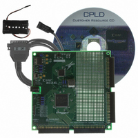
Manufacturer Part Number
DO-CPLD-DK-G
Description
KIT DESIGN CPLD W/BATT HOLDER
Manufacturer
Xilinx Inc
Series
CoolRunner™- IIr
Type
CPLDr
Specifications of DO-CPLD-DK-G
Contents
Proto Board, Download Cable, Samples, Software
For Use With/related Products
CoolRunner-ll, XC9500XL
Lead Free Status / RoHS Status
Lead free / RoHS Compliant
Other names
122-1512
Available stocks
Company
Part Number
Manufacturer
Quantity
Price


Implementing FPGA Designs
Introduction
Programmable Logic Design
June 12, 2006
R
Implementing an FPGA design is a slightly different process than implementing a CPLD
design. The FPGA uses Map, Place and Route instead of Fit. Mapping includes tools
for floorplanning and manual placing and routing.
As with a CPLD, after you have successfully simulated your design, the synthesis stage
converts the code-based HDL or schematic-based design into an NGC netlist file. The
netlist is a non-readable file that describes the actual circuit to be implemented at a very
low level.
The implementation phase uses the netlist and a constraints file to recreate the design
using the available resources within the FPGA. Constraints may be physical or timing and
are commonly used for setting the required frequency of the design or declaring the
required pin-out.
The map stage distributes the design to the resources available in the FPGA. Obviously, if
the design is too big for the specified device, mapping will be incomplete. The map stage
also uses the UCF file to understand timing and may sometimes decide to add further logic
(replication) to meet the given timing requirements. Map has the ability to “shuffle’ the
design around LUTs to create the best possible implementation for the design. The whole
process is automatic and requires little user input.
The place and route stage works with the allocated CLBs and chooses the best location for
each block. For a fast logic path, it makes sense to place relevant CLBs next to each other
simply to minimize the path length. The routing resources are then allocated to each
connection, again using a careful selection of the best possible routing types. For example,
if you need a signal for many areas of the design, the place and route tool would use a
“longline” to span the chip with minimal delay or skew.
After running place and route, it is good practice to re-simulate. As all of the logic delays
added by the LUTs and flip-flops are now known (as well as the routing delays), the
chosen simulator can use this information for timing simulation.
Finally, a program called “bitgen” takes the output of place and route and creates a
programming bitstream. When developing a design, it may not be necessary to create a bit
file on every implementation, as you may only need to ensure that a particular portion of
your design passes timing verification.
The steps of implementation must be carried out in this order:
1.
2.
3.
4.
Synthesize
Map
Place and Route
Timing Simulate
www.xilinx.com
Chapter 6
Introduction
103
Related parts for DO-CPLD-DK-G
Image
Part Number
Description
Manufacturer
Datasheet
Request
R

Part Number:
Description:
STARTER KIT CPLD
Manufacturer:
Xilinx Inc
Datasheet:
Part Number:
Description:
KIT STARTER CPLD JAPANESE
Manufacturer:
Xilinx Inc
Datasheet:
Part Number:
Description:
KIT STARTER CPLD-JAPANESE
Manufacturer:
Xilinx Inc
Datasheet:

Part Number:
Description:
IC CPLD .8K 36MCELL 44-VQFP
Manufacturer:
Xilinx Inc
Datasheet:

Part Number:
Description:
IC CPLD 72MCRCELL 10NS 44VQFP
Manufacturer:
Xilinx Inc
Datasheet:

Part Number:
Description:
IC CPLD 1.6K 72MCELL 64-VQFP
Manufacturer:
Xilinx Inc
Datasheet:

Part Number:
Description:
IC CR-II CPLD 64MCELL 44-VQFP
Manufacturer:
Xilinx Inc
Datasheet:

Part Number:
Description:
IC CPLD 1.6K 72MCELL 100-TQFP
Manufacturer:
Xilinx Inc
Datasheet:

Part Number:
Description:
IC CR-II CPLD 64MCELL 56-BGA
Manufacturer:
Xilinx Inc
Datasheet:

Part Number:
Description:
IC CPLD 72MCRCELL 7.5NS 44VQFP
Manufacturer:
Xilinx Inc
Datasheet:
Part Number:
Description:
IC CR-II CPLD 64MCELL 100-VQFP
Manufacturer:
Xilinx Inc
Datasheet:
Part Number:
Description:
IC CPLD 1.6K 72MCELL 100-TQFP
Manufacturer:
Xilinx Inc
Datasheet:

Part Number:
Description:
IC CPLD 72MCRCELL 7.5NS 64VQFP
Manufacturer:
Xilinx Inc
Datasheet:
Part Number:
Description:
IC CPLD 1.6K 72MCELL 100-TQFP
Manufacturer:
Xilinx Inc
Datasheet:

Part Number:
Description:
IC CPLD 1.5K 64MCELL HP 44-VQFP
Manufacturer:
Xilinx Inc