DO-CPLD-DK-G Xilinx Inc, DO-CPLD-DK-G Datasheet - Page 55
DO-CPLD-DK-G
Manufacturer Part Number
DO-CPLD-DK-G
Description
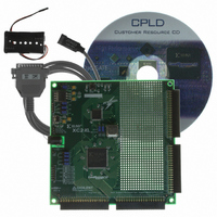
KIT DESIGN CPLD W/BATT HOLDER
Manufacturer
Xilinx Inc
Series
CoolRunner™- IIr
Type
CPLDr
Specifications of DO-CPLD-DK-G
Contents
Proto Board, Download Cable, Samples, Software
For Use With/related Products
CoolRunner-ll, XC9500XL
Lead Free Status / RoHS Status
Lead free / RoHS Compliant
Other names
122-1512
Available stocks
Company
Part Number
Manufacturer
Quantity
Price


Programmable Logic Design
June 12, 2006
R
Downloading or Programming
can compensate for an ill-conceived architecture, especially if there are not enough routing
tracks. If you were to encounter this problem, the most common solution would be to use
a larger device. And you would likely remember the experience the next time you selected
a vendor.
A related program is called timing-driven place and route (TDPR). This allows you to specify
timing criteria that will be used during device layout. A static timing analyzer is usually part
of the vendor’s implementation software. It provides timing information about paths in
the design. This information is very accurate and can be viewed in many different ways,
such as displaying all paths in the design and ranking them from longest to shortest delay.
In addition, at this point you can use the detailed layout information after reformatting
and go back to your chosen simulator with detailed timing information. This process is
called back-annotation and has the advantage of providing the accurate timing as well as the
zeros and ones operation of your design. In both cases, the timing reflects delays of the
logic blocks as well as the interconnect. The final implementation step is the download or
program.
Download generally refers to volatile devices such as SRAM FPGAs. As the name implies,
you download the device configuration information into the device memory. The
bitstream that is transferred contains all the information to define the logic and
interconnect of the design and is different for every design. Because SRAM devices lose
their configuration when the power is turned off, the bitstream must be stored somewhere
for a production solution. A common such place is a serial PROM. There is an associated
piece of hardware that connects from the computer to a board containing the target device.
Program is used to program all non-volatile programmable logic devices, including serial
PROMs. Programming performs the same function as download, except that the
configuration information is retained after the power is removed from the device. For
antifuse devices, programming can only be done once per device – hence the term one-
time programmable. Programming of Xilinx CPLDs can be done in-system via JTAG or
with a conventional device programmer such as Data I/O. JTAG Boundary Scan –
formally known as IEEE/ANSI standard 1149.1_1190 – is a set of design rules that facilitate
testing, device programming, and debugging at the chip, board, and system levels.
www.xilinx.com
HDL Design Process
45
Related parts for DO-CPLD-DK-G
Image
Part Number
Description
Manufacturer
Datasheet
Request
R

Part Number:
Description:
STARTER KIT CPLD
Manufacturer:
Xilinx Inc
Datasheet:
Part Number:
Description:
KIT STARTER CPLD JAPANESE
Manufacturer:
Xilinx Inc
Datasheet:
Part Number:
Description:
KIT STARTER CPLD-JAPANESE
Manufacturer:
Xilinx Inc
Datasheet:

Part Number:
Description:
IC CPLD .8K 36MCELL 44-VQFP
Manufacturer:
Xilinx Inc
Datasheet:

Part Number:
Description:
IC CPLD 72MCRCELL 10NS 44VQFP
Manufacturer:
Xilinx Inc
Datasheet:

Part Number:
Description:
IC CPLD 1.6K 72MCELL 64-VQFP
Manufacturer:
Xilinx Inc
Datasheet:

Part Number:
Description:
IC CR-II CPLD 64MCELL 44-VQFP
Manufacturer:
Xilinx Inc
Datasheet:

Part Number:
Description:
IC CPLD 1.6K 72MCELL 100-TQFP
Manufacturer:
Xilinx Inc
Datasheet:

Part Number:
Description:
IC CR-II CPLD 64MCELL 56-BGA
Manufacturer:
Xilinx Inc
Datasheet:

Part Number:
Description:
IC CPLD 72MCRCELL 7.5NS 44VQFP
Manufacturer:
Xilinx Inc
Datasheet:
Part Number:
Description:
IC CR-II CPLD 64MCELL 100-VQFP
Manufacturer:
Xilinx Inc
Datasheet:
Part Number:
Description:
IC CPLD 1.6K 72MCELL 100-TQFP
Manufacturer:
Xilinx Inc
Datasheet:

Part Number:
Description:
IC CPLD 72MCRCELL 7.5NS 64VQFP
Manufacturer:
Xilinx Inc
Datasheet:
Part Number:
Description:
IC CPLD 1.6K 72MCELL 100-TQFP
Manufacturer:
Xilinx Inc
Datasheet:

Part Number:
Description:
IC CPLD 1.5K 64MCELL HP 44-VQFP
Manufacturer:
Xilinx Inc